
Three-dimensional packaging structure and method for bonding wall fan-out device

A three-dimensional packaging and wall structure technology, applied in the direction of electric solid devices, semiconductor devices, assembling microstructure devices, etc., can solve the problems of small chip area, difficult to meet product requirements, too many I/Os, etc. Device area, ease of processing, effect of increasing device count

Pending Publication Date: 2020-01-24
XIAMEN SKY SEMICON TECH CO LTD
View PDF1 Cites 3 Cited by
  • Summary
  • Abstract
  • Description
  • Claims
  • Application Information

AI Technical Summary

Problems solved by technology

With the further improvement of chip integration and the further increase of the number of I / Os, it is difficult for traditional wafer-level packaging (WLCSP) to meet product requirements, and it is necessary to solve the contradiction between too many I / Os and too small chip area in WLCSP

Method used


Image

  • Three-dimensional packaging structure and method for bonding wall fan-out device
  • Three-dimensional packaging structure and method for bonding wall fan-out device
  • Three-dimensional packaging structure and method for bonding wall fan-out device

Examples


Embodiment Construction

[0043] The present invention will be further described below through specific embodiments.

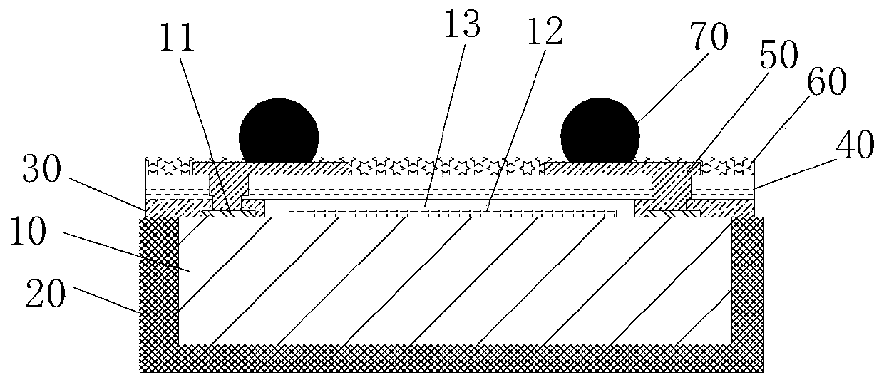
[0044] refer to figure 1 , a three-dimensional packaging structure for bonded wall fan-out devices, including a device 10, an encapsulation material 20, a wall structure 30, a cover plate 40, a metal interconnection structure, and the like. The first surface of the device 10 is provided with pads 11 and functional areas 12 . The functional area 12 is provided with an IDT, and the pad 11 can be an aluminum pad, an AlNiAu pad, an AlNiPdAu pad, and the like. The chip type of the device of the present invention is a SAW filter, a BAW filter or other filter devices with similar functions, and the device 10 is a device 10 after dicing wafer materials such as lithium niobate, lithium tantalate, glass, and silicon.

[0045] The encapsulation material 20 encapsulates the device 10 except the first surface, see figure 1 , the encapsulation material 20 encapsulates four sides and one bottom ed...


PUM


Abstract

The invention discloses a three-dimensional packaging structure and method for a bonding wall fan-out device. The first surface of the device is provided with a functional area and a plurality of bonding pads. The three-dimensional packaging structure is characterized in that all surfaces of the device, except the first surface, are provided with an encapsulating material; a wall structure is prepared on the first surface of the device and extends to the first surface of the encapsulating material; the wall structure partially covers at least one bonding pad, and first openings are formed at the bonding pads respectively; a cover plate is arranged to be bonded to the wall structure, so that a cavity structure is formed in the functional area of the device; and at least one second opening communicated with the first openings is formed in the cover plate; and the surface of the cover plate is provided with metal interconnection structures which are electrically connected with the bondingpads through the first openings and the second openings. With the three-dimensional packaging structure and method for the bonding wall fan-out device of the invention adopted, overall structure reliability can be improved, risks are reduced, and cost is reduced.

Description

technical field [0001] The invention relates to the field of semiconductor packaging, in particular to a three-dimensional packaging structure and method for bonding wall fan-out devices. Background technique [0002] For many MEMS, such as accelerometers, RF switches, gyroscopes, and various sensors, such as filters, CMOS image sensors, it is necessary to form a protective cavity to protect the device and provide a vacuum or airtight working environment for the device . With the development of technology, the size of the chip is getting smaller and smaller, and for many devices, such as SAW filters and CMOS image sensors, the sealing wall cannot be set on the surface of the device, so the size of the wall used to form the cavity is getting smaller and smaller. The narrower, the reduction of the bonding area has a great impact on the bonding force and the reliability of the device. New low-cost, high-reliability solutions must be found. [0003] Fan-out packaging technolo...

Claims


Application Information

Patent Timeline
Patent Type & Authority Applications(China)
IPC IPC(8): H01L23/31H01L25/065H03H9/25B81B7/02B81C1/00
CPCH01L23/3128H01L25/0655B81B7/02H03H9/25B81C1/00269B81C2203/01B81C2203/0109H01L2224/11H01L23/3114H01L21/561H03H9/1071H03H9/1014H01L21/8213H01L23/29H01L23/49816H01L24/04H01L2224/04105
Inventor 于大全
Owner XIAMEN SKY SEMICON TECH CO LTD
Learn More