Manufacturing method of multilayer flexible circuit board and manufactured product

A technology for flexible circuit boards and manufacturing methods, applied in multilayer circuit manufacturing, printed circuit manufacturing, circuit substrate materials, etc., can solve the problem of increased power consumption and signal transmission loss, large dielectric constant and loss factor, and poor structural characteristics etc. to achieve low power consumption and high-frequency signal transmission loss, improve production and processing efficiency, and improve signal transmission performance

Inactive Publication Date: 2020-01-10
李龙凯
View PDF0 Cites 3 Cited by
  • Summary
  • Abstract
  • Description
  • Claims
  • Application Information

AI Technical Summary

Problems solved by technology

At present, polyimide (PI) is mainly used as the substrate of flexible boards. However, due to the large dielectric constant and loss factor of PI substrates, large moisture absorption, and poor reliability, the PI flexible boards The high-frequency transmission loss is serious and the structural characteristics are poor, which can no longer adapt to the current high-frequency and high-speed trend
Therefore, with the emergence of new 5G technology products, the signal transmission frequency and speed of existing circuit boards have been difficult to meet the requirements of 5G technology products
[0004] At the same time, in the preparation process of traditional multi-layer flexible circuit boards, there are generally many technical processes, complicated production, and problems such as increased power consumption and signal transmission loss in terms of circuit board performance.
[0005] At the same time, when the precision circuit board is powered on, copper ions will migrate between the lines. During the use of the equipment, the circuit will burn and explode due to conduction and collision, resulting in circuit The wiring on the board is not safe and working properly

Method used


Image

  • Manufacturing method of multilayer flexible circuit board and manufactured product
  • Manufacturing method of multilayer flexible circuit board and manufactured product
  • Manufacturing method of multilayer flexible circuit board and manufactured product

Examples


Embodiment Construction

[0041] In order to further illustrate the technical means and functions adopted by the present invention to achieve the intended purpose, the specific implementation modes of the present invention will be described in detail below in conjunction with the accompanying drawings and preferred embodiments.

[0042] An embodiment of the present invention provides a method for manufacturing a multilayer flexible circuit board, including the following steps:

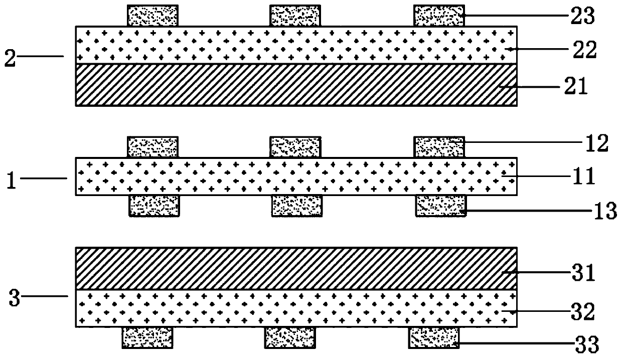
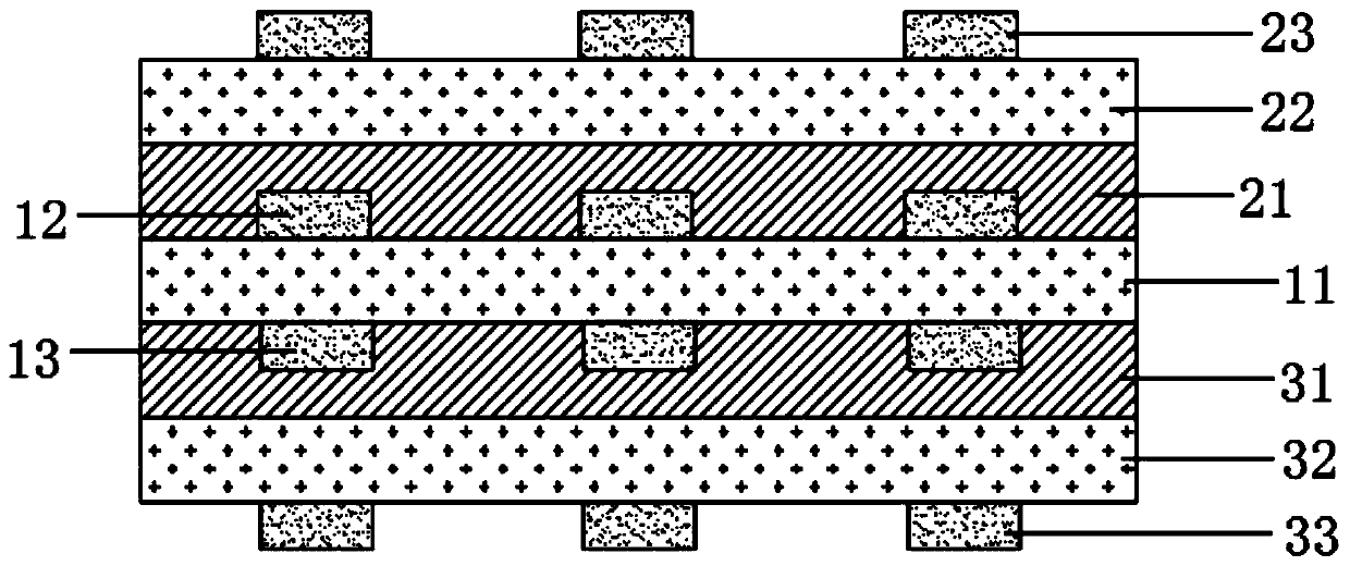
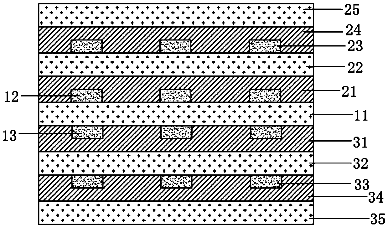
[0043] (1) Making a double-sided FPC flexible board: apply a copper layer on the upper and lower surfaces of the base film, and form a circuit on the copper layer to obtain a double-sided FPC flexible board;

[0044] (2) Make at least one set of new material layer structures

[0045] (2.1) Apply a copper layer on the first surface of the film to form a single panel;

[0046] (2.2) Apply a semi-cured high-frequency material layer on the other surface of the single-sided film to obtain at least one set of new material layer stru...


PUM


Abstract

The invention discloses a manufacturing method of a multilayer flexible circuit board. The manufacturing method comprises the steps of (1) manufacturing a double-sided FPC flexible board; (2) manufacturing a novel material layer structure; (3) hot-pressing at least one group of novel material layer structures on the circuit on the upper surface and / or the lower surface of the double-sided FPC flexible board, and forming a protective layer on the circuit of the outermost novel material layer structure and / or the exposed circuit of the double-sided FPC flexible board to obtain the multi-layer flexible circuit board. The invention further discloses a multi-layer flexible circuit board manufactured by implementing the method. According to the invention, the manufacturing process is simplifiedand convenient, and the production efficiency is high; the manufactured multi-layer flexible circuit board not only greatly simplifies the novel material layer structure and reduces the overall thickness, but also has the function of transmitting high-frequency signals at a high speed, and is particularly suitable for novel 5G technological products; the protective and resistant effects on the copper ion migration phenomenon during the electrification between the circuits are achieved, and the safe and normal work of the circuits is guaranteed.

Description

technical field [0001] The invention relates to the field of circuit boards, in particular to a method for manufacturing a multilayer flexible circuit board and products thereof. Background technique [0002] At present, from the communication network to the terminal application, the communication frequency is comprehensive and high-frequency, and high-speed and large-capacity applications emerge in endlessly. In recent years, with the transition of wireless networks from 4G to 5G, network frequencies have continued to increase. According to the 5G development roadmap shown in relevant materials, the future communication frequency will be upgraded in two stages. The goal of the first stage is to increase the communication frequency to 6GHz before 2020, and the goal of the second stage is to further increase it to 30-60GHz after 2020. In terms of market applications, the signal frequency of terminal antennas such as smartphones continues to increase, and there are more and ...

Claims


Application Information

Patent Timeline
Patent Type & Authority Applications(China)
IPC IPC(8): H05K3/46H05K3/00H05K1/03H05K1/02
CPCH05K3/4611H05K3/0011H05K1/036H05K1/0313H05K1/0216H05K1/028H05K3/4626H05K3/4632H05K2203/068Y02D30/70H05K3/4673H05K2201/0195H05K1/0393H05K2203/1105
Inventor 李龙凯
Owner 李龙凯
Why Eureka
Try Eureka