


Quick Research
Generate reliable direction feasibility study reports for your R&D in just a few steps.

Technical Q&A
Discover and master advanced knowledge NOW. Basics, ideas, possibilities, all at once.

Find Solutions
As an expert in R&D theories, this can generate solutions to your technical problems instantly.

Evaluate Feasibility
Analyze your overall solution with one click, know your potential R&D risks in advance.

Monitor Landscape
Get weekly tech updates, stay abreast of the latest tech innovations and key insights.
Manufacturing method of multi-fold mask layer
A manufacturing method and mask layer technology, which can be applied to the photolithographic process of the patterned surface, semiconductor/solid-state device manufacturing, and originals for photomechanical processing, etc., can solve the problem of low precision and difficult Further narrow the gap and other issues
- Summary
- Abstract
- Description
- Claims
- Application Information
AI Technical Summary
Problems solved by technology
Method used
Image

Examples
Embodiment 1
[0113] like Figures 7 to 19 As shown, this embodiment provides a method for fabricating a multiple mask layer, and the fabrication method includes:
[0114] like Figures 7 to 8 As shown, step 1) is first performed, a substrate 201 is provided, a first mask layer 203 is formed on the substrate 201, the first mask layer 203 includes a plurality of imaging mask units 2031, and the imaging mask There is an imaging gap 204 on the substrate 201 between the film units 2031, and the size of the imaging mask unit 2031 depends on the minimum exposure development size capability.
[0115] The substrate 201 includes a layer to be etched, and the layer to be etched may be a semiconductor substrate material, a dielectric material, a metal material, or various stacked materials composed of the above materials.
[0116] The material of the first mask layer 203 includes one selected from the group consisting of photoresist, silicon dioxide, silicon nitride, silicon oxynitride and polysilic...
Embodiment 2
[0146] like Figure 20 to Figure 33 As shown, this embodiment provides a method for fabricating a multiple mask layer, and the fabrication method includes:
[0147] like Figure 20 ~ Figure 21 As shown, step 1) is first performed, a substrate 201 is provided, a first mask layer 203 is formed on the substrate 201, the first mask layer 203 includes a plurality of imaging mask units 2031, and the imaging mask There are imaging gaps 204 on the substrate 201 between the film units 2031 .
[0148] The substrate 201 includes a layer to be etched, and the layer to be etched may be a semiconductor substrate material, a dielectric material, a metal material, or various stacked materials composed of the above materials.
[0149] The material of the first mask layer 203 includes one selected from the group consisting of photoresist, silicon dioxide, silicon nitride, silicon oxynitride and polysilicon. In this embodiment, the material of the first mask layer 203 can be selected as photo...
Embodiment 3
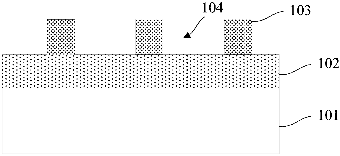
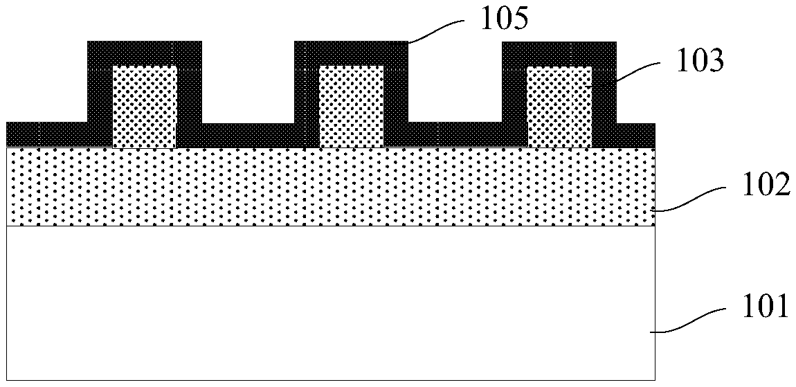
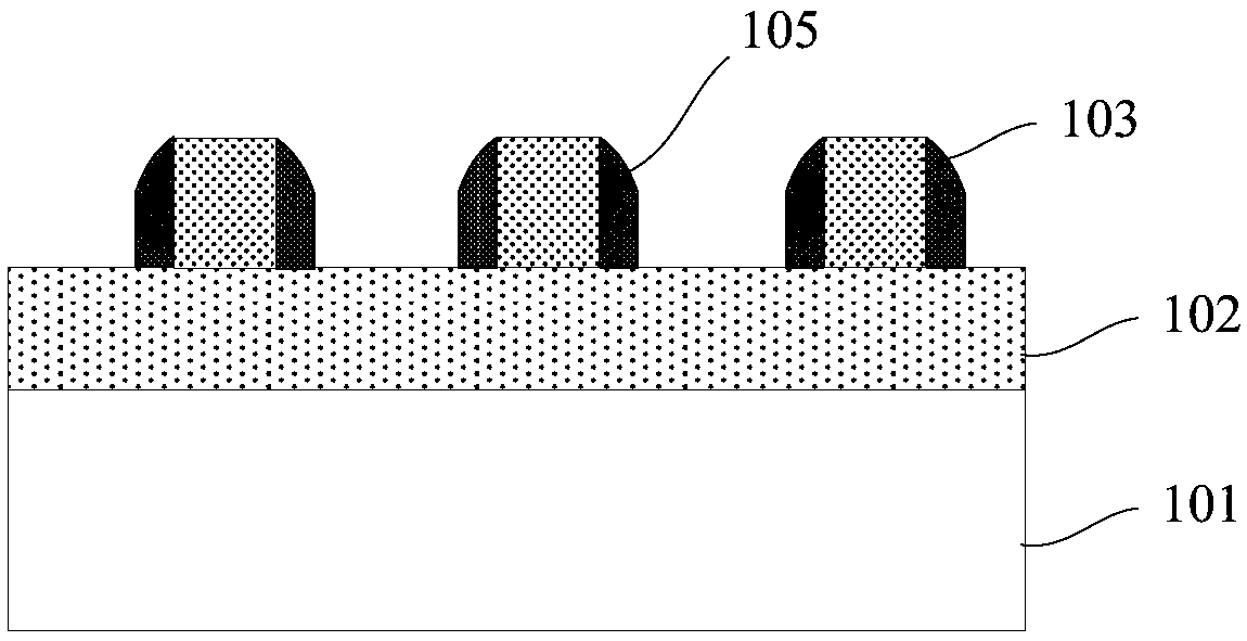
[0181] like Figure 34 to Figure 48 As shown, this embodiment provides a method for fabricating a multiple mask layer, and the fabrication method includes:
[0182] like Figure 34 to Figure 35 As shown, step 1) is first performed, a substrate 201 is provided, a bottom mask layer 202 is formed on the substrate 201, a first mask layer 203 is formed on the bottom mask layer 202, and the first mask Layer 203 includes a plurality of imaging mask units 2031 with imaging gaps 204 on the bottom mask layer 202 therebetween.
[0183] The substrate 201 includes a layer to be etched, and the layer to be etched may be a semiconductor substrate material, a dielectric material, a metal material, or various stacked materials composed of the above materials.
[0184] The material of the first mask layer 203 includes one selected from the group consisting of photoresist, silicon dioxide, silicon nitride, silicon oxynitride and polysilicon. In this embodiment, the material of the first mask la...
PUM
 Abstract
Description
Claims
Application Information
 - R&D Engineer
- R&D Manager
- IP Professional
- Industry Leading Data Capabilities
- Powerful AI technology
- Patent DNA Extraction
Browse by: Latest US Patents, China's latest patents, Technical Efficacy Thesaurus, Application Domain, Technology Topic, Popular Technical Reports.
© 2024 PatSnap. All rights reserved.Legal|Privacy policy|Modern Slavery Act Transparency Statement|Sitemap|About US| Contact US: help@patsnap.com