A kind of preparation method of high transmittance buffer layer structure for transparent electrode of laminated battery
A transparent electrode, high transmittance technology, applied in circuits, electrical components, photovoltaic power generation, etc., can solve the problems of poor light transmittance of thin-layer metal, complicated preparation of silver nanowires, poor repeatability, etc., and achieves many and simple deposition methods. , Protect the transparent organic interface layer, a variety of effects
- Summary
- Abstract
- Description
- Claims
- Application Information
AI Technical Summary
Problems solved by technology
Method used
Image
Examples
Embodiment 1
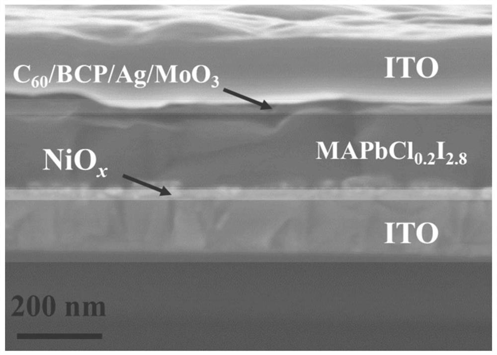
[0029] Ag is generated by in situ chemical reaction 2 MoO 4 Preparation of perovskite transparent cells as a buffer layer.
[0030] (1) The commercially purchased indium tin oxide (ITO) glass was first cleaned with detergent, and then ultrasonically cleaned with tap water, deionized water, ethanol, acetone, and isopropanol in sequence.
[0031] (2) After drying the ITO, spin-coat a 30 nm-thick hole transport layer NiO for use.
[0032] (3) Preparation of 250 nm thick CH on the NiO layer 3 NH 3 PbCl 0.2 I 2.8 perovskite layer.
[0033] (4) In vacuum (-4 Pa) Evaporation at 40 nm C 60 as the electron transport layer, after C 60 10 nm BCP was evaporated on top as a barrier layer.
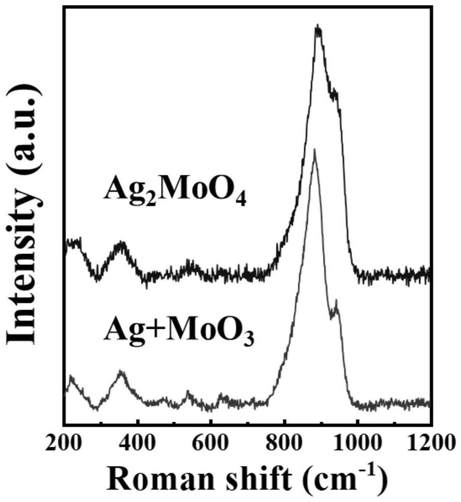
[0034] (5) On BCP, in vacuum (-4 In the Pa) environment, 1 nm Ag was first evaporated, and the evaporation current was 35A. Then 3 nm MoO was evaporated on Ag 3 , the evaporation temperature is 450~550℃, and the current is 1.8~2.6A. in high vacuum (-4 Pa) and high temperature (>100 °C), Ag a...
Embodiment 2
[0039] Ag is generated by in situ chemical reaction 2 MoO 4 Preparation of perovskite transparent cells as a buffer layer.
[0040] (1) The commercially purchased indium tin oxide (ITO) glass was first cleaned with detergent, and then ultrasonically cleaned with tap water, deionized water, ethanol, acetone, and isopropanol in sequence.
[0041] (2) After drying the ITO, spin-coat a 30 nm-thick hole transport layer NiO for use.
[0042] (3) Preparation of 250 nm thick CH on the NiO layer 3 NH 3 PbCl 0.2 I 2.8 perovskite layer.
[0043] (4) In vacuum (-4 Pa) Evaporation at 40 nm C 60 as the electron transport layer, after C 60 10 nm BCP was evaporated on top as a barrier layer.
[0044] (5) On BCP, in vacuum (-4 In the Pa) environment, 3 nm Ag was first evaporated, and the evaporation current was 40A. Then 1 nm MoO was evaporated on Ag 3 , the evaporation temperature is 450 ℃, and the current is 2A. in high vacuum (-4 Pa) and high temperature (>100℃), Ag atoms deposi...
Embodiment 3
[0048] Ag is generated by in situ chemical reaction 2 MoO 4 Preparation of perovskite transparent cells as a buffer layer.
[0049] (1) The commercially purchased indium tin oxide (ITO) glass was first cleaned with detergent, and then ultrasonically cleaned with tap water, deionized water, ethanol, acetone, and isopropanol in sequence.
[0050] (2) After drying the ITO, spin-coat a 30 nm-thick hole transport layer NiO for use.
[0051] (3) Preparation of 250 nm thick CH on the NiO layer 3 NH 3 PbCl 0.2 I 2.8 perovskite layer.
[0052] (4) In vacuum (-4 Pa) Evaporation at 40 nm C 60 as the electron transport layer, after C 60 10 nm BCP was evaporated on top as a barrier layer.
[0053] (5) On BCP, in vacuum (-4 In the Pa) environment, 5 nm Ag was first evaporated, and the evaporation current was 45 A. Then 20nm MoO was evaporated on Ag 3 , the evaporation temperature is 450~600 ℃, and the current is 2~3 A. in high vacuum (-4 Pa) and high temperature (>100 °C), Ag at...
PUM
| Property | Measurement | Unit |
|---|---|---|
| thickness | aaaaa | aaaaa |
| thickness | aaaaa | aaaaa |
| thickness | aaaaa | aaaaa |
Abstract
Description
Claims
Application Information
 - R&D
- Intellectual Property
- Life Sciences
- Materials
- Tech Scout
- Unparalleled Data Quality
- Higher Quality Content
- 60% Fewer Hallucinations
Browse by: Latest US Patents, China's latest patents, Technical Efficacy Thesaurus, Application Domain, Technology Topic, Popular Technical Reports.
© 2025 PatSnap. All rights reserved.Legal|Privacy policy|Modern Slavery Act Transparency Statement|Sitemap|About US| Contact US: help@patsnap.com


