Multilayer ultra-wideband wave-absorbing body based on electric loss material and magnetic material combination
A technology of magnetic materials and wave absorbers, applied in the direction of electrical components, antennas, etc., can solve the problems that the absorption strength and absorption width are difficult to meet the requirements, the reflection curve fluctuates violently, and the low-frequency absorption effect is not good.
- Summary
- Abstract
- Description
- Claims
- Application Information
AI Technical Summary
Problems solved by technology
Method used
Image
Examples
Embodiment 1
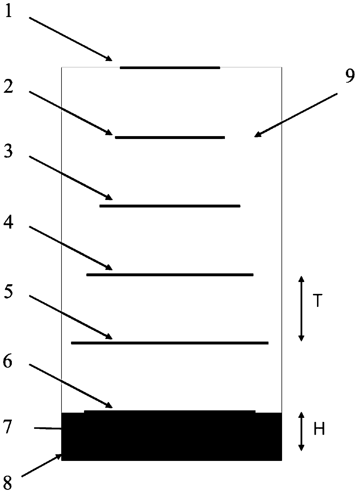
[0027] Such as figure 1 As shown, by designing a multilayer resistive film with variable size and resistance value on the magnetic absorption layer, the electromagnetic wave in the broadband range is incident into the material and absorbed by the loss; the resistive film plays the role of absorbing electromagnetic waves and adjusting impedance matching. The absorption effect is further enhanced by the high loss of the bottom magnetic material. By rationally designing and optimizing the unit structure, a strong electromagnetic resonance in the broadband range is achieved, and an ultra-broadband absorbing effect is obtained. The absorption of low frequencies is mainly due to the magnetic loss of magnetic materials.
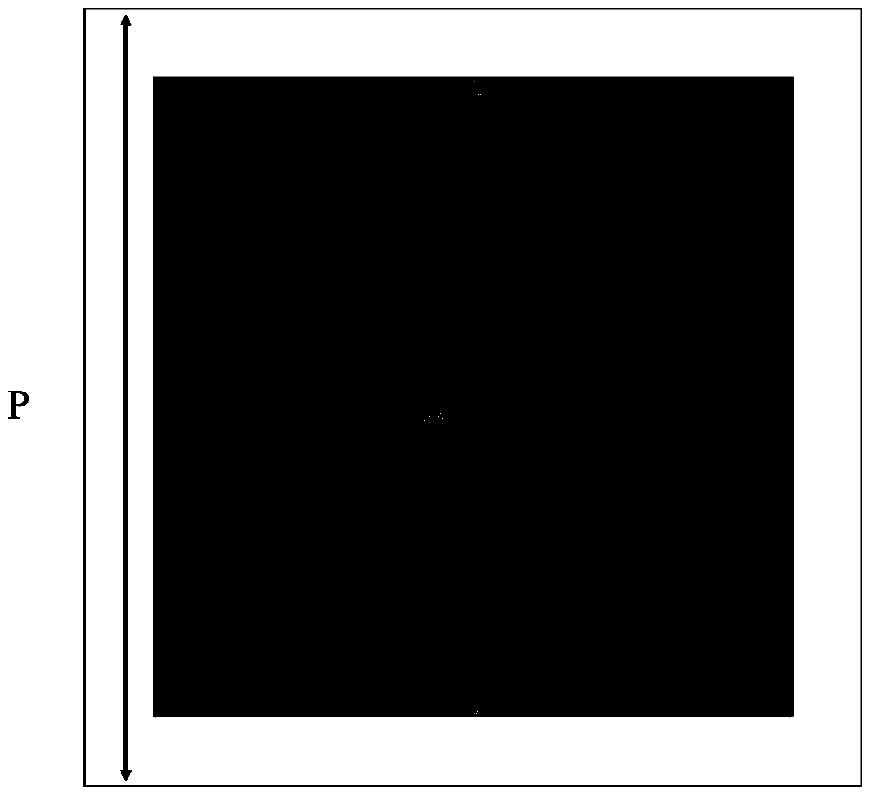
[0028] Such as figure 2 As shown, the ultra-broadband absorbing structure consists of a first resistive film layer (1), a second resistive film layer (2), a third resistive film layer (3), a fourth resistive film layer (4), a fifth resistive film layer The film ...
Embodiment 2
[0039] The support layer (9) spaced by the resistive film adopts a honeycomb material with a similar dielectric constant, and the relative dielectric constant ε1 is 1.15; the honeycomb material has higher compressive strength than the foam material. The honeycomb and the resistance film can also be bonded together by an adhesive through the adhesive film, and the adhesive can be epoxy resin, polyester resin, polyacrylic resin, etc.;
[0040] The square resistance Rs=60-200Ω / sq of each layer resistance film, the resistance film distance T=4mm; Unit period p=15mm; The cell size L1=5.0mm of the first layer resistance film (1), the second layer resistance film ( 2) unit size L2=6.8mm, the unit size L3=8.5mm of the third layer resistance film (3), the unit size L4=10.2mm of the fourth layer resistance film (4), the fifth layer resistance film (5) The cell size L5=12.0mm, the cell size L6=10.0mm of the sixth layer of resistance film (6).
[0041] Figure 6The reflection curve in i...
PUM
| Property | Measurement | Unit |
|---|---|---|
| Square resistance | aaaaa | aaaaa |
| Thickness | aaaaa | aaaaa |
| Thickness | aaaaa | aaaaa |
Abstract
Description
Claims
Application Information
 - R&D
- Intellectual Property
- Life Sciences
- Materials
- Tech Scout
- Unparalleled Data Quality
- Higher Quality Content
- 60% Fewer Hallucinations
Browse by: Latest US Patents, China's latest patents, Technical Efficacy Thesaurus, Application Domain, Technology Topic, Popular Technical Reports.
© 2025 PatSnap. All rights reserved.Legal|Privacy policy|Modern Slavery Act Transparency Statement|Sitemap|About US| Contact US: help@patsnap.com


