Reverse bias type silicon light-emitting SOI optoelectronic isolator, integrated circuit thereof and manufacturing method
A technology of photoelectric isolator and manufacturing method, which is applied in the direction of circuits, electrical components, semiconductor devices, etc., and can solve the problems of high manufacturing cost, increased manufacturing difficulty, and difficult dispensing and spot welding processes
- Summary
- Abstract
- Description
- Claims
- Application Information
AI Technical Summary
Problems solved by technology
Method used
Image
Examples
Embodiment 1
[0070] Example 1 A reverse-biased silicon light-emitting SOI photoelectric isolator
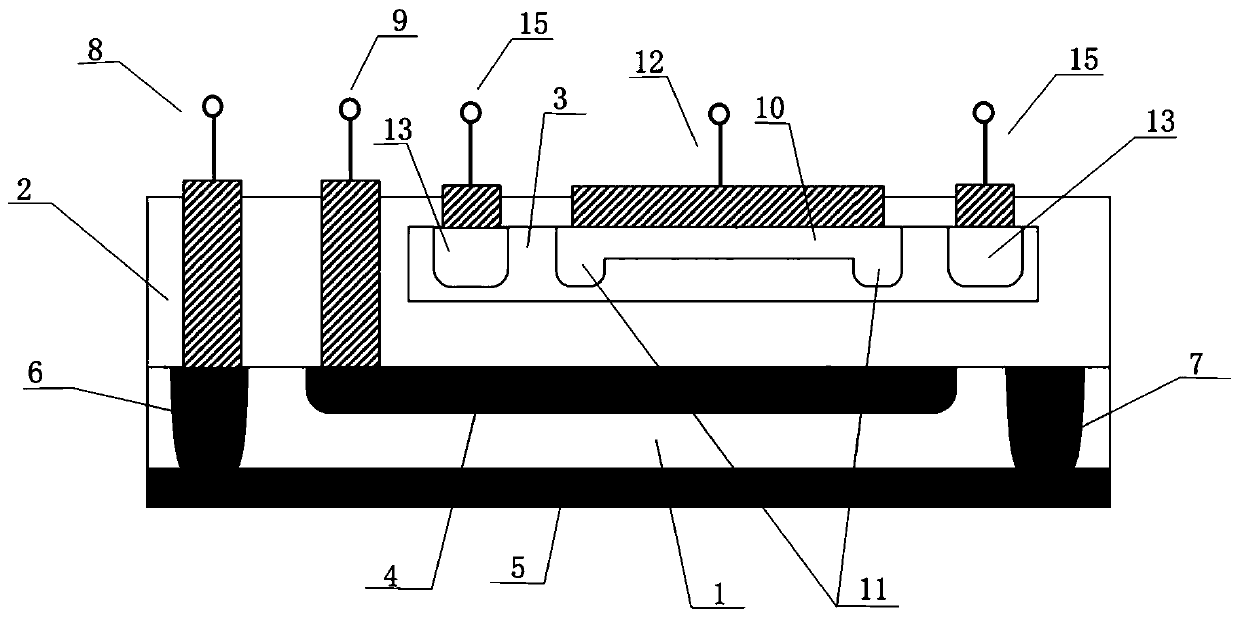
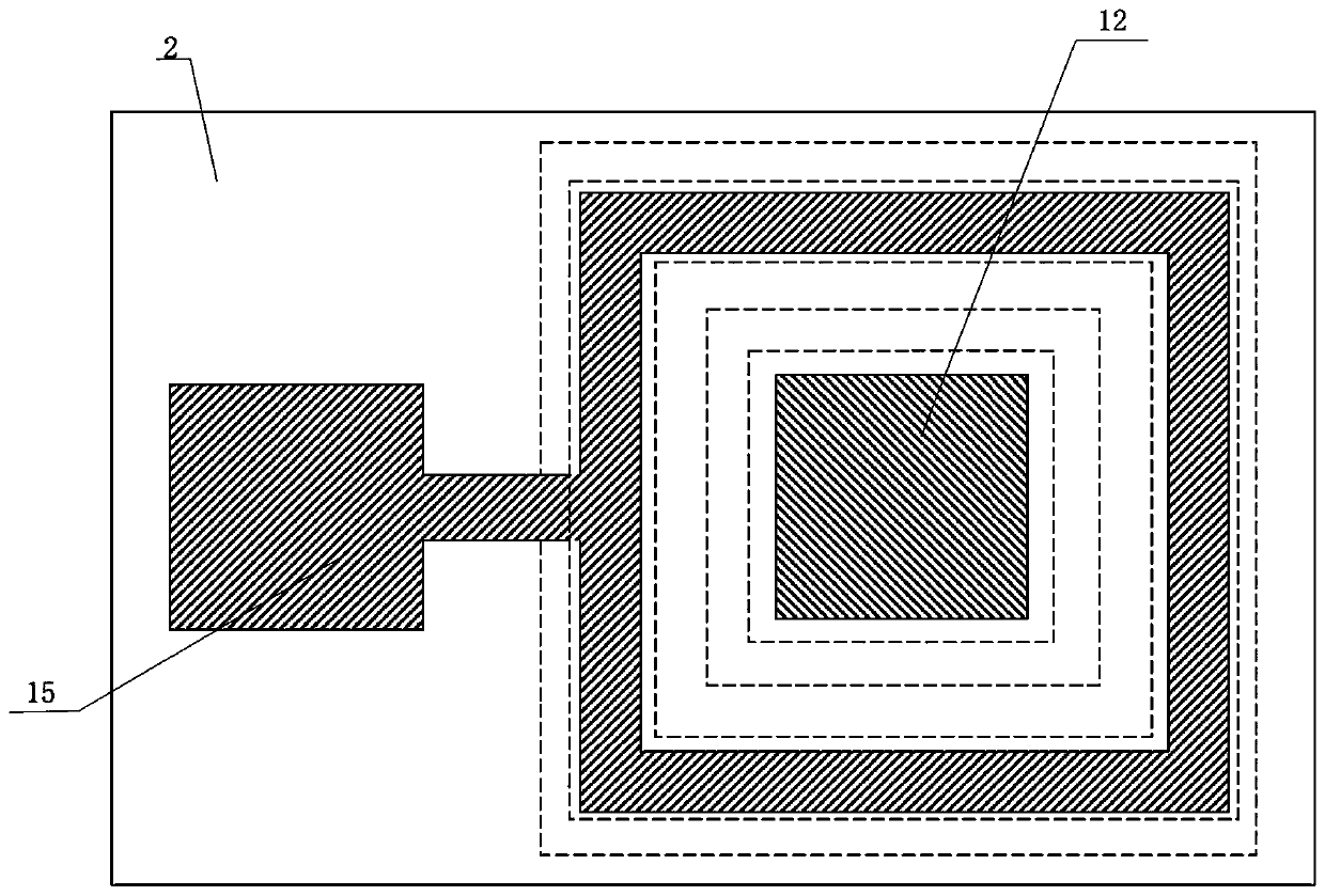
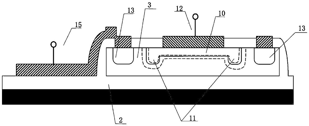
[0071] like Figure 1-Figure 3 As shown, this embodiment includes n - Doped first substrate 1, as SiO 2 The first dielectric layer 2 and the top layer of silicon 3 in the middle layer, the first substrate 1 and the top layer of silicon 3 are bonded by intelligent lift-off technology; The detector, the first dielectric layer 2 and the silicon light source fabricated in the top layer of silicon 3; the first substrate 1 is n - doping / p - A doped silicon substrate, the first substrate 1 is implanted with a first deep p-well 5 and connected with the first deep p-well 5 to form a first island with a first high aspect ratio p + Well 6 and the second high aspect ratio p + Well 7, the upper part of the first island is embedded with a first thin n + well 4; silicon photodetector cathode 8 from the first high aspect ratio p + Well 6 lead out, silicon photodetector anode 9 from the first thin n +...
Embodiment 2
[0076] Example 2 A reverse-biased silicon light-emitting SOI photoelectric isolator
[0077] The difference between this embodiment and embodiment 1 is that, as Figure 4 and Figure 5 As shown, the top layer of silicon 3 is a p-type doped silicon film, and the top layer of silicon 3 is embedded with seven spaced and interconnected n + The well consists of a zigzag n + well, sawtooth n + The well divides the p-type doped silicon film into eight inner zigzag p-wells that are spaced apart and communicated with each other.
[0078] from zigzag n + The positive electrode 12 of the light source is drawn from the well, and the negative electrode 15 of the light source is drawn from the inner zigzag p-well; Figure 4 and Figure 5 The wiring method of the silicon light source is given.
[0079] In fact, n + The number of wells can be determined according to actual needs. In this embodiment, seven wells are taken as an example for illustration.
Embodiment 3
[0080] Example 3 A manufacturing method of a reverse-biased silicon light-emitting SOI opto-isolator
[0081] This embodiment is used to make embodiment 1, and proceeds according to the following steps:
[0082] One, choose n - doping / p - The doped first silicon wafer is used as the first substrate 1. After the surface of the first substrate 1 is cleaned, the first deep p-well is sequentially completed on the first substrate 1 by means of a mask plate using an ion implantation process. 5. The first high aspect ratio p + Well 6, the second high aspect ratio p + The manufacture of the well 7 forms the first island, and then embeds the first thin n on the upper part of the first island + Well 4;
[0083] 2. Growth of the first SiO with a thickness of 300nm-500nm on the first substrate 1 by the low-pressure chemical vapor deposition method 2 Layer, in order to play the role of electrical isolation;
[0084] 3. Select the second silicon wafer, and implant H into the second s...
PUM
| Property | Measurement | Unit |
|---|---|---|
| Thickness | aaaaa | aaaaa |
| Thickness | aaaaa | aaaaa |
Abstract
Description
Claims
Application Information
 - Generate Ideas
- Intellectual Property
- Life Sciences
- Materials
- Tech Scout
- Unparalleled Data Quality
- Higher Quality Content
- 60% Fewer Hallucinations
Browse by: Latest US Patents, China's latest patents, Technical Efficacy Thesaurus, Application Domain, Technology Topic, Popular Technical Reports.
© 2025 PatSnap. All rights reserved.Legal|Privacy policy|Modern Slavery Act Transparency Statement|Sitemap|About US| Contact US: help@patsnap.com


