Manufacturing method of interlayer film

A manufacturing method and interlayer film technology, applied in semiconductor/solid-state device manufacturing, electrical components, circuits, etc., can solve problems affecting device performance, metal residue, cost increase, etc., to avoid electrical performance, eliminate metal residue, no The effect of metal residue

Active Publication Date: 2019-11-19
SHANGHAI HUALI INTEGRATED CIRCUTE MFG CO LTD
View PDF5 Cites 1 Cited by
  • Summary
  • Abstract
  • Description
  • Claims
  • Application Information

AI Technical Summary

Problems solved by technology

[0027] However, by Figure 1H As shown, it can be seen that metal residues will be generated in the region of the cavity 302a, as indicated by marks 109a and 110a
[0028] At the same time, due to the presence of butterfly defects formed by the concave surface of the interlayer film 108, there will also be metal residues at the butterfly defects.
[0029] Residual metal obviously affects device performance
In order to eliminate the influence of residual metal, the only way is to perform CMP to thin the interlayer film 108 and the metal gate 110, but this is prone to the risk of exposure of the embedded silicon germanium layer 108 , the exposure of the embedded silicon germanium layer 108 will adversely affect the electrical performance of the semiconductor device
At the same time, the increased CMP to eliminate residual metals also increases the cost

Method used


Image

  • Manufacturing method of interlayer film
  • Manufacturing method of interlayer film
  • Manufacturing method of interlayer film

Examples


Embodiment Construction

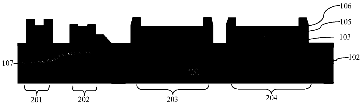
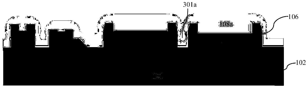
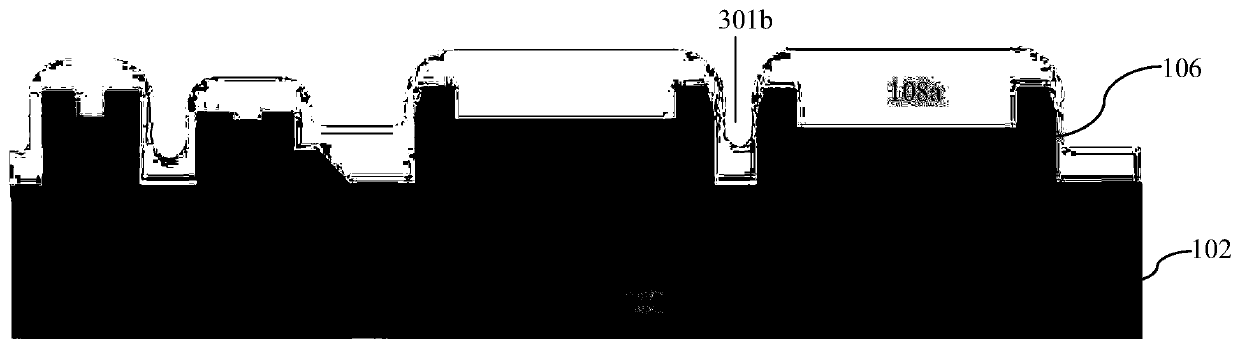
[0060] Such as figure 2 Shown is the flow chart of the manufacturing method of the interlayer film in the embodiment of the present invention; as Figure 3A to Figure 3D As shown, it is a device structure diagram in each step of the method of the embodiment of the present invention. The method for manufacturing the interlayer film of the embodiment of the present invention includes the following steps:

[0061] Step 1, such as Figure 3A As shown, a semiconductor substrate 1 is provided, on which pattern structures of semiconductor devices are formed, and the regions between the pattern structures are pattern spacers.

[0062] In the embodiment of the present invention, the semiconductor substrate 1 is a silicon substrate.

[0063] The semiconductor device is a MOS transistor with HKMG. The interlayer film is the zeroth interlayer film. Usually, the semiconductor device will form multiple layers of metal, wherein the metal layers of each layer need to be isolated by an in...


PUM


Abstract

The invention discloses a manufacturing method of an interlayer film. The method comprises the following steps of step1, providing a semiconductor substrate forming a pattern structure; step2, using afirst insulating layer which has a high filling ability and is formed through a first growth technology to fill a pattern interval region and extending the first insulating layer to an outer portionof the pattern interval region, and forming a closed cavity while filling; step3, taking a pattern structure as an end point of grinding to carry out first chemical mechanical grinding, forming a dishing defect in a pattern structure region and at the same time, opening a cavity; step4, forming a second insulating layer by using a second growth technology, using the second insulating layer to completely fill the cavity, wherein hardness of the second insulating layer is higher than the hardness of the first insulating layer; and step5, taking the pattern structure as the end point of grindingto carry out second chemical mechanical grinding, and eliminating the dishing defect by using a characteristic that the hardness of the second insulating layer is increased. In the invention, the cavity formed through filling an interlayer film in the pattern interval region can be eliminated, and the dishing defect on an interlayer film surface of a top of the pattern interval region can be reduced or eliminated.

Description

technical field [0001] The invention relates to a method for manufacturing a semiconductor integrated circuit, in particular to a method for manufacturing an interlayer film. Background technique [0002] Such as Figure 1A to Figure 1H As shown, it is a device structure diagram in each step of the manufacturing method of the existing interlayer film, and the manufacturing method of the existing interlayer film includes the following steps: [0003] Step 1, such as Figure 1A As shown, a semiconductor substrate 101 is provided, on which pattern structures of semiconductor devices are formed, and the regions between the pattern structures are pattern spacers. [0004] Usually, the semiconductor substrate 101 is a silicon substrate. [0005] The semiconductor device is a MOS transistor with HKMG. HKMG has a gate dielectric layer with a high dielectric constant (HK) and a metal gate (MG), so it is usually abbreviated as HKMG in the art. [0006] The interlayer film 108 is t...

Claims


Application Information

Patent Timeline
Patent Type & Authority Applications(China)
IPC IPC(8): H01L21/768H01L21/3105H01L21/8238
CPCH01L21/76819H01L21/31053H01L21/823871
Inventor 孙敏强李昱廷陈建勋胡展源
Owner SHANGHAI HUALI INTEGRATED CIRCUTE MFG CO LTD
Why Eureka
Try Eureka