a kind of aggas 2 Base intermediate band semiconductor material and preparation method thereof
A semiconductor and intermediate zone technology, applied in the field of AgGaS2-based intermediate zone semiconductor materials and their preparation, can solve the problems of low dispersion, lack of semiconductor materials, and inability to meet the requirements of high-efficiency solar cells, and achieves enhanced light absorption and increased electron light absorption paths. , Improve the effect of photoelectric conversion efficiency
- Summary
- Abstract
- Description
- Claims
- Application Information
AI Technical Summary
Problems solved by technology
Method used
Image
Examples
Embodiment 1
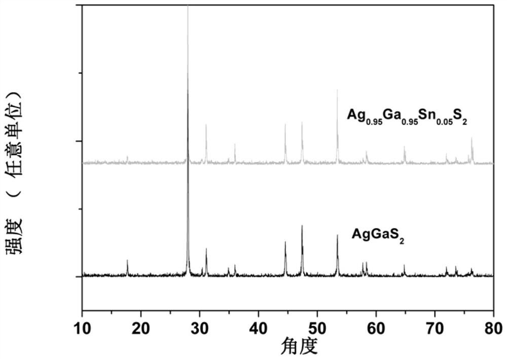
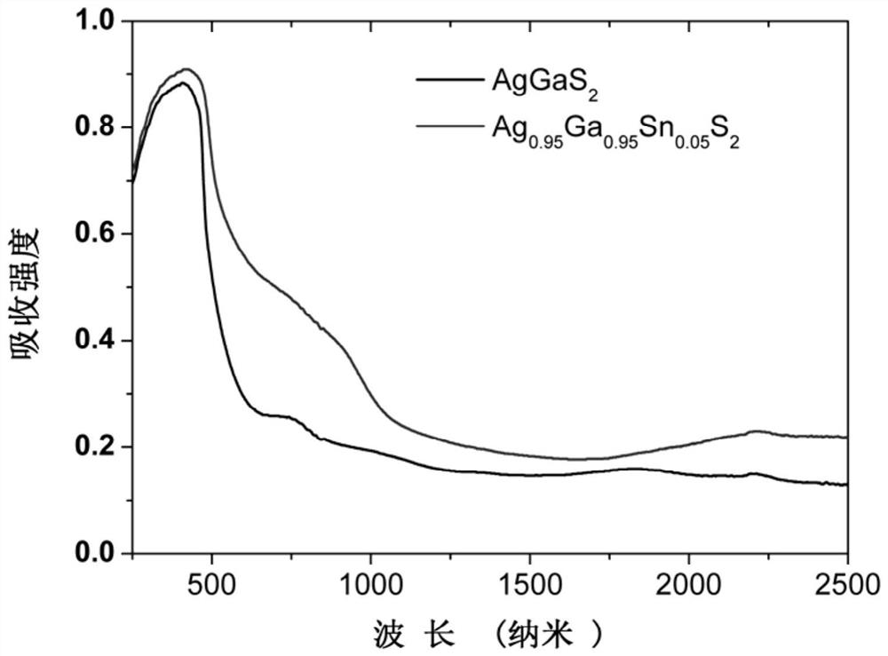
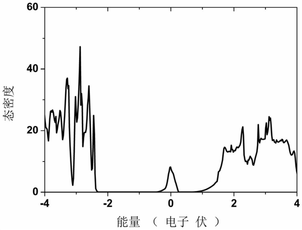
[0031] AgGaS 2 It is a compound with a chalcopyrite structure, and it has a good light-absorbing ability, and is suitable as a parent compound for high-efficiency intermediate-band semiconductor materials. In this embodiment, AgGaS with excellent photoelectric performance 2 It is the parent semiconductor of the intermediate band, and the intrinsic semiconductor AgGaS is doped with the group VI element Sn 2 Ga sites, introducing an intermediate impurity band into the band gap of the intrinsic semiconductor can effectively improve the AgGaS 2 The optical absorption ability makes it have better optical absorption and improves AgGaS 2 Comprehensive performance of semiconductors in the field of solar cells.
[0032] The electronic density of states was calculated using the first-principles calculation method. AgGaS 2 It is a chalcopyrite structure compound with 16 atoms in the tetragonal unit cell. The doping calculation model adopts a 2×2×2 supercell model, which contains 64...
Embodiment 2
[0046] a AgGaS 2 A method for preparing a base intermediate band semiconductor material, specifically comprising the following steps:
[0047] (1) Ag powder, Ga block, S powder and Sn powder (all with a purity of 5N) are vacuum-packaged in a quartz glass tube according to the stoichiometric ratio;
[0048] (2) Carry out primary sintering of the quartz glass tube, the temperature of the primary sintering is 800°C, and the sintering time is 80 hours. The obtained primary sintered sample is ground and vacuum-packed in the quartz glass tube again;
[0049] (3) The quartz glass tube is subjected to secondary sintering, the temperature of the secondary sintering is 800°C, and the sintering time is 80 hours, and the obtained secondary sintered sample is ground to obtain the product AgGa 1-x sn x S 2 (x=0.01).
[0050] The quartz glass tubes in step (2) and step (3) are sintered in a muffle furnace, and ground in an agate mortar.
Embodiment 3
[0052] a AgGaS 2 A method for preparing a base intermediate band semiconductor material, specifically comprising the following steps:
[0053] (1) Ag powder, Ga block, S powder and Sn powder (all with a purity of 5N) are vacuum-packaged in a quartz glass tube according to the stoichiometric ratio;
[0054] (2) Carry out primary sintering of the quartz glass tube, the temperature of the primary sintering is 900°C, and the sintering time is 60 hours, and the obtained primary sintered sample is ground and re-vacuum-packed in the quartz glass tube;
[0055] (3) The quartz glass tube is subjected to secondary sintering, the temperature of the secondary sintering is 900°C, and the sintering time is 60 hours, and the obtained secondary sintered sample is ground to obtain the product AgGa 1-x sn x S 2 (x=0.04).
[0056] The quartz glass tubes in step (2) and step (3) are sintered in a muffle furnace, and ground in an agate mortar.
PUM
| Property | Measurement | Unit |
|---|---|---|
| purity | aaaaa | aaaaa |
| purity | aaaaa | aaaaa |
Abstract
Description
Claims
Application Information
 - R&D Engineer
- R&D Manager
- IP Professional
- Industry Leading Data Capabilities
- Powerful AI technology
- Patent DNA Extraction
Browse by: Latest US Patents, China's latest patents, Technical Efficacy Thesaurus, Application Domain, Technology Topic, Popular Technical Reports.
© 2024 PatSnap. All rights reserved.Legal|Privacy policy|Modern Slavery Act Transparency Statement|Sitemap|About US| Contact US: help@patsnap.com


