Preparation method of antimony selenide thin-film solar cell
A solar cell, antimony selenide technology, applied in circuits, photovoltaic power generation, electrical components, etc., can solve the problems of not being suitable for wide application and industrial production, process repeatability of waste liquid pollution, and other impurities, etc., and achieve low environmental impact. , less time, stable performance
- Summary
- Abstract
- Description
- Claims
- Application Information
AI Technical Summary
Problems solved by technology
Method used
Image
Examples
preparation example Construction
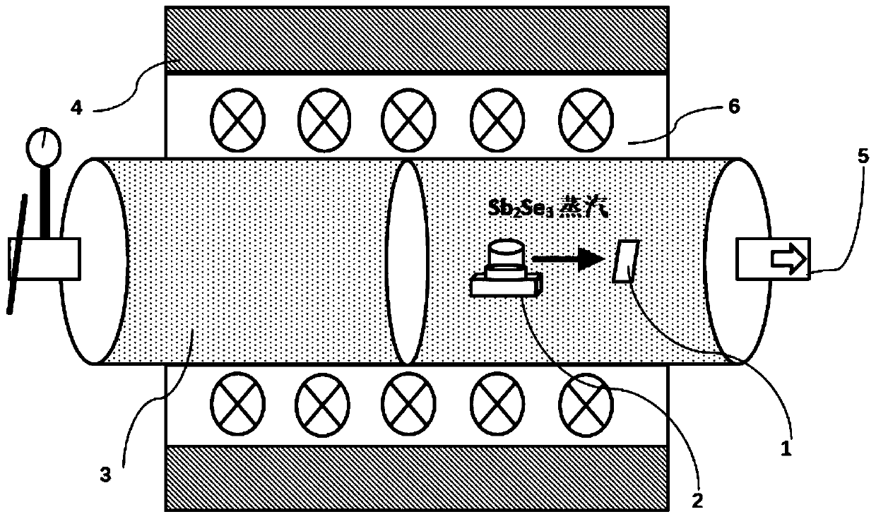
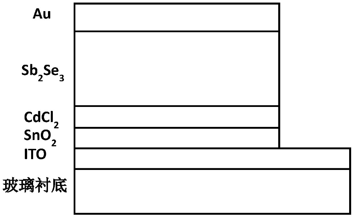
[0030] The preparation method of a kind of antimony selenide thin-film solar cell of the present invention, at first dispose tin oxide hydrocolloid dispersion liquid and cadmium chloride aqueous solution of certain mass ratio, secondly on the clean patterned ITO conductive glass, spin in turn by spin coating method Coating and preparing tin oxide electron transport layer and cadmium chloride modification layer, drying and heat treatment, as the substrate, place the weighed antimony selenide powder and the substrate in the corresponding position of the quartz tube; then vacuumize the chamber , heat up the atmosphere furnace at a lower temperature (close to room temperature) at a certain heating rate. After reaching a certain temperature, keep it warm for a few minutes, and immediately open the upper cover of the atmosphere furnace after the heat preservation is over, so that the cavity can be cooled down to room temperature quickly, and the substrate Take it out, complete the fi...
Embodiment 1
[0044] 1) First, disperse 1 g of directly purchased tin oxide hydrocolloid dispersion into 4 g of deionized water, vibrate and sonicate for 20 minutes to obtain a tin oxide hydrocolloid dispersion with a mass ratio of 1:4.
[0045] 2) Weigh 0.1g of cadmium chloride powder and dissolve it in 5g of deionized water, stir for 5min to obtain a cadmium chloride aqueous solution with a mass ratio of 0.1:5.
[0046] 3) On a clean patterned ITO conductive glass (the area of the glass substrate is 2×2cm 2 ), prepare a layer of tin oxide electron transport layer with a thickness of 50-60nm by spin coating method, the spin coating parameter is 3000r / min, coat for 30s and then place it on a hot plate at 150°C for 30min to obtain a uniform and smooth tin oxide film .
[0047] 4) On the tin oxide electron transport layer, spin coating with a speed of 800r / min for 5s by spin coating method, and then spin coating with a speed of 2500r / min for 20s to prepare a cadmium chloride modification l...
Embodiment 2
[0052] 1) First, disperse 1 g of directly purchased tin dioxide hydrocolloid dispersion into 5 g of deionized water, vibrate and sonicate for 20 minutes to obtain a tin dioxide gel dispersion with a mass ratio of 1:5.
[0053] 2) Weigh 0.1g of cadmium chloride powder and dissolve it in 5g of deionized water, stir for 5min to obtain a cadmium chloride aqueous solution with a mass ratio of 0.1:5.
[0054] 3) On a clean patterned ITO conductive glass (the area of the glass substrate is 2×2cm 2 ), prepare a layer of tin dioxide electron transport layer with a thickness of 50-60nm by spin coating method, the spin coating parameter is 3000r / min, coat for 30s and then place it on a hot plate at 150°C for 30min to obtain a uniform and smooth tin dioxide tin film.
[0055] 4) On the tin dioxide electron transport layer, spin coating at a rate of 800r / min for 5s by spin coating method, and then spin coating at a rate of 2500r / min for 20s to prepare a cadmium chloride modification lay...
PUM
 Abstract
Description
Claims
Application Information
 - R&D
- Intellectual Property
- Life Sciences
- Materials
- Tech Scout
- Unparalleled Data Quality
- Higher Quality Content
- 60% Fewer Hallucinations
Browse by: Latest US Patents, China's latest patents, Technical Efficacy Thesaurus, Application Domain, Technology Topic, Popular Technical Reports.
© 2025 PatSnap. All rights reserved.Legal|Privacy policy|Modern Slavery Act Transparency Statement|Sitemap|About US| Contact US: help@patsnap.com


