Molded article for joining and method for producing the same

A molded body and bonding strength technology, applied in semiconductor/solid-state device manufacturing, manufacturing tools, welding equipment, etc., can solve the problem of difficult high-strength semiconductor chip components being bonded to the substrate

Active Publication Date: 2021-11-12
MITSUBISHI MATERIALS CORP
View PDF4 Cites 0 Cited by
  • Summary
  • Abstract
  • Description
  • Claims
  • Application Information

AI Technical Summary

Problems solved by technology

[0005] However, regarding the Cu core Sn shell powder molded body described in Non-Patent Document 1, when a natural oxide film is formed on the surface of the Cu core Sn shell powder before molding, even if the molded body is placed on a semiconductor as a member to be joined Reflow is performed between the chip component and the substrate, and it is difficult for the Sn of the casing to infiltrate the surface of the Cu particles, and it is difficult to bond the semiconductor chip component to the substrate with high strength.

Method used


Image

  • Molded article for joining and method for producing the same
  • Molded article for joining and method for producing the same
  • Molded article for joining and method for producing the same

Examples


Embodiment 1

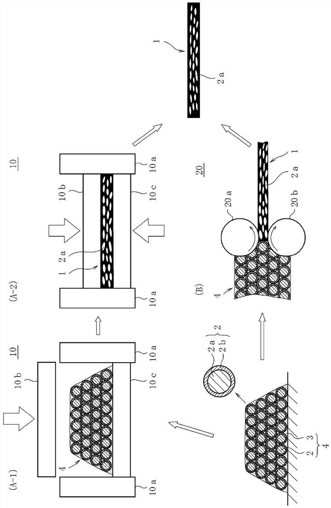
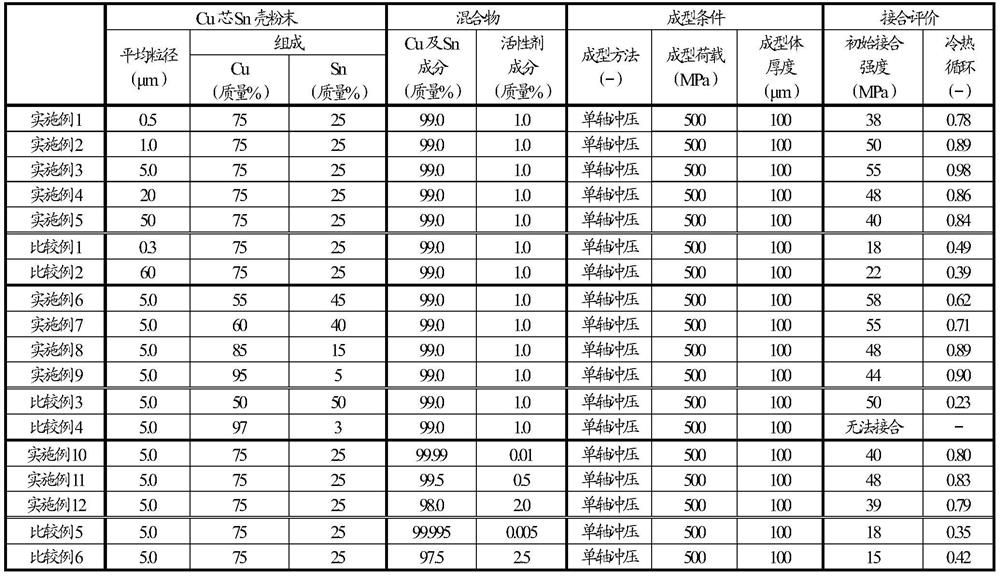
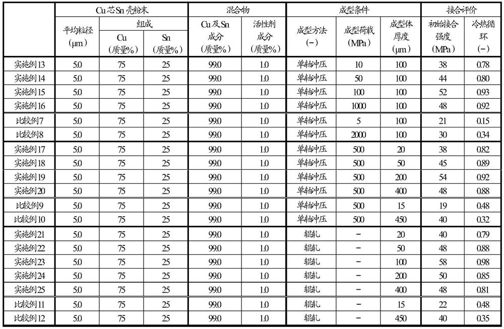
[0034]A Cu core Sn shell powder having an average particle diameter of 0.5 μm, a Cu ratio of 75% by mass, and a Sn ratio of 25% by mass was prepared. Here, the compositional ratio of Cu and Sn in the Cu core Sn shell powder was measured by ICP emission spectroscopy (manufactured by Thermo Fisher Scientific, iCAP-6500Duo). In addition, the crystal structure of the core-shell structure is mainly composed of Cu and Sn, and was confirmed by a powder X-ray diffraction method (manufactured by PANalytical, multi-purpose X-ray diffractometer Empyrean). Next, under a nitrogen atmosphere, the Cu core Sn shell powder was put in a mortar, a general-purpose flux (92MS manufactured by Arakawa Chemical Industries, Ltd.) was added to the Cu core Sn shell powder, and uniformly mixed for 30 minutes to obtain a mixture. In this mixture, the gaps between the Cu core Sn shell powders, that is, the inner walls of the closed cells and the open cells are covered with the active agent content. In the...

Embodiment 2~5 and comparative example 1、2

[0036] In Examples 2 to 5 and Comparative Examples 1 and 2, as shown in Table 1, the average particle diameter of the Cu core Sn shell powder used to produce the molded body for joining was used. The Cu core Sn shell powder was used in the same manner as in Example 1 to obtain a molded body for joining.

Embodiment 6~9 and comparative example 3、4

[0038] In Examples 6 to 9 and Comparative Examples 3 and 4, as shown in Table 1, Cu and Sn compositions different from those in Example 1 were used for the composition of Cu and Sn of the Cu core Sn shell powder used to make the molded body for joining. Cu-core-Sn-shell powder having a Sn composition was obtained in the same manner as in Example 1 to obtain a molded body for joining.


PUM

PropertyMeasurementUnit
particle sizeaaaaaaaaaa
thicknessaaaaaaaaaa
particle diameteraaaaaaaaaa

Abstract

The present invention is a molded body for joining (1) composed of an aggregate of compressed Cu-core Sn-shell powder, and an active agent content ( 3) The activator-containing material (3) is used to remove oxides on the surface of the powder, and the molded body for joining contains Cu in a ratio of 55 to 95% by mass and Sn in a ratio of 45 to 5% by mass. The active agent in the active agent-containing material is contained in a ratio of 0.01 to 2 mass % with respect to 100 mass % of the molded body for joining, and the thickness of the molded body for joining is 20 to 400 μm.

Description

technical field [0001] The present invention relates to a molded body for bonding which is interposed between electronic components such as semiconductor chip elements and LED chip elements as members to be bonded and a substrate, and which is suitable for use when mounting electronic components as members to be bonded on a substrate, and its Production method. In addition, this international application claims priority based on Japanese Patent Application No. 71961 (Japanese Patent Application No. 2017-71961) filed on March 31, 2017, and the entire contents of Japanese Patent Application No. 2017-71961 are used in this international application . Background technique [0002] In recent years, wide bandgap semiconductors such as SiC that can operate at high temperatures exceeding 200° C. have attracted attention. As a bonding method for semiconductor chip elements that operate at high temperatures, a bonding method called Transient Liquid Phase Sintering (TLP method) in wh...

Claims


Application Information

Patent Timeline
Patent Type & Authority Patents(China)
IPC IPC(8): B23K35/14B22F1/00B22F1/02B23K35/26B23K35/40B22F1/17
CPCB23K35/40B23K35/0244B23K35/262B23K35/302B22F2003/1106B22F3/11B22F7/002B22F2998/10B22F2999/00H01L23/142H01L21/4871B22F1/17B22F3/02B22F3/18B22F2201/10B22F2201/02C22C9/10
Inventor 樋上晃裕村冈弘树岩田广太郎山口朋彦
Owner MITSUBISHI MATERIALS CORP
Why Eureka
Try Eureka