Composite cooling positive electrode-based GaN planar gunn diode and fabrication method thereof

A Gunn diode and anode technology is applied in the field of GaN planar Gunn diodes and their preparation based on composite heat dissipation anodes. The effect of reducing the self-heating effect

Inactive Publication Date: 2019-10-18
NORTHWESTERN POLYTECHNICAL UNIV
View PDF6 Cites 1 Cited by
  • Summary
  • Abstract
  • Description
  • Claims
  • Application Information

AI Technical Summary

Problems solved by technology

In the isothermal energy balance model (EB mode), the electronic domain is a dipole domain mode, corresponding to the maximum power output; while in the non-isothermal energy balance model (NEB mode), the electronic domain decays into a dipole domain-accumulation domain transition mode , to further increase the voltage and intensify the self-heating effect, the electronic domains are completely attenuated into accumulation domain modes, and the output power is greatly reduced

Method used


Image

  • Composite cooling positive electrode-based GaN planar gunn diode and fabrication method thereof
  • Composite cooling positive electrode-based GaN planar gunn diode and fabrication method thereof
  • Composite cooling positive electrode-based GaN planar gunn diode and fabrication method thereof

Examples


Embodiment 1

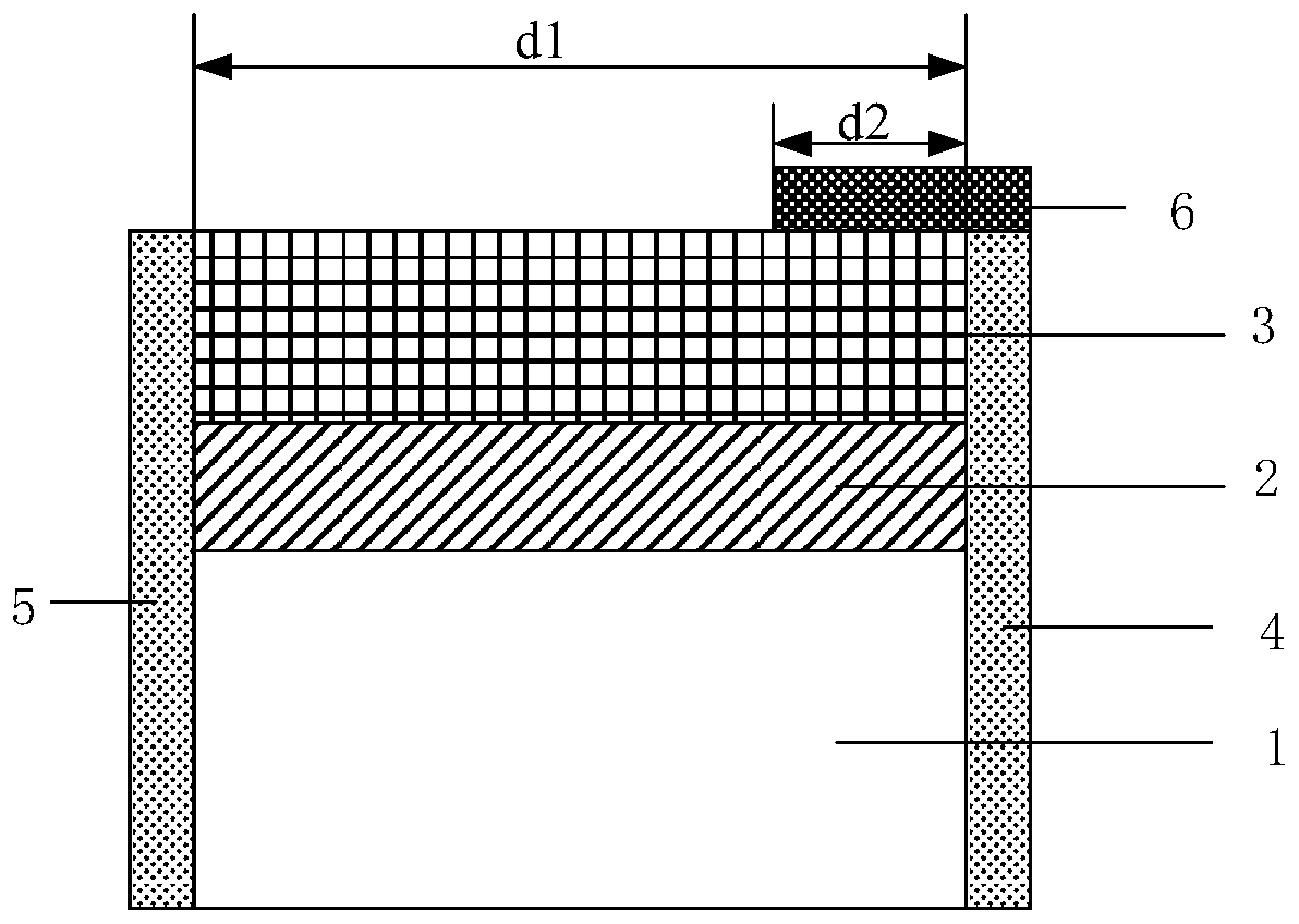
[0042] See figure 2 , figure 2 The schematic diagram of the structure of the first GaN planar Gunn diode based on the compound heat dissipation anode provided by the embodiment of the present invention. The planar Gunn diode includes an AlGaN back barrier layer 1 , a GaN channel layer 2 , an AlGaN barrier layer 3 , an ohmic contact anode 4 , an ohmic contact cathode 5 and a Schottky extension layer 6 .

[0043] Among them, the GaN channel layer 2 is located on the AlGaN back barrier layer 1; the AlGaN barrier layer 3 is located on the GaN channel layer 2; the ohmic contact anode 4 is located on the AlGaN back barrier layer 1, the GaN channel layer 2 and the AlGaN barrier layer One end of the layer 3, the ohmic contact cathode 5 is located at the other end of the AlGaN back barrier layer 1, the GaN channel layer 2 and the AlGaN barrier layer 3; the Schottky extension layer 6 is located on the AlGaN barrier layer 3 and covers the ohmic contact on anode 4.

[0044]In order t...

Embodiment 2

[0055] On the basis of Example 1, please refer to Figure 5 , Figure 5 A schematic diagram of the structure of the second GaN planar Gunn diode based on the compound heat dissipation anode provided by the embodiment of the present invention. The planar Gunn diode includes: an AlGaN back barrier layer 1 , a GaN channel layer 2 , an AlGaN barrier layer 3 , an ohmic contact anode 4 , an ohmic contact cathode 5 , a heat dissipation film 7 and a Schottky extension layer 6 .

[0056] Wherein, the GaN channel layer 2 is located on the AlGaN back barrier layer 1 , and the AlGaN barrier layer 3 is located on the GaN channel layer 2 . The ohmic contact anode 4 is located at one end of the GaN channel layer 2 and the AlGaN barrier layer 3 , and the ohmic contact cathode 5 is located at the other end of the GaN channel layer 2 and the AlGaN barrier layer 3 . The heat dissipation film 7 is located on the surface of the AlGaN barrier layer 3 and covers the ohmic contact anode 4 , and the...

Embodiment 3

[0063] See Figure 9 , Figure 9 A schematic diagram of the structure of the fourth GaN planar Gunn diode based on the compound heat dissipation anode provided by the embodiment of the present invention, Figure 9 The GaN planar Gunn diode includes: AlGaN back barrier layer 1, GaN channel layer 2, AlGaN barrier layer 3, ohmic contact anode 4, ohmic contact cathode 5 and Schottky extension layer 6.

[0064] Wherein, the AlGaN barrier layer 3 is located on the GaN channel layer 2 . The ohmic contact anode 4 is located at one end of the surface of the AlGaN barrier layer 3 , and the ohmic contact cathode 5 is located at the other end of the surface of the AlGaN barrier layer 3 . The Schottky extension layer 6 is located on the surface of the AlGaN barrier layer 3 and covers the ohmic contact anode 4, and together with the ohmic contact anode 4 forms a composite heat dissipation anode to suppress the self-heating effect of the device. For the relevant features of the Schottky e...


PUM

PropertyMeasurementUnit
thicknessaaaaaaaaaa

Abstract

The invention relates to a composite cooling positive electrode-based GaN planar gunn diode and a fabrication method thereof. The planar gunn diode comprises an AlGaN back barrier layer, a GaN channellayer, an AlGaN barrier layer, an ohmic contact positive electrode, an ohmic contact negative electrode and a Schottky extension layer, wherein the GaN channel layer is arranged on the AlGaN back barrier layer, the AlGaN barrier layer is arranged on the GaN channel layer, the ohmic contact positive electrode and the ohmic contact negative electrode are respectively arranged at two ends of the AlGaN back barrier layer, the GaN channel layer and the AlGaN barrier layer, and the Schottky extension layer is arranged on the AlGaN barrier layer and covers the ohmic contact positive electrode. The Schottky extension layer of the planar gunn diode forms a depletion layer in a channel of the planar gunn diode, the strength of high-energy dipole domain is reduced, so that the energy of electronic domain is dispersed, the collision ionization of a positive electrode end of the planar gunn diode is reduced, heat generation is buffered, the self-heating effect of a device is further effectively prevented, and the negative resistance effect, the power and the frequency of the device are improved.

Description

technical field [0001] The invention belongs to the field of semiconductors, and in particular relates to a GaN planar Gunn diode based on a composite heat dissipation anode and a preparation method thereof. Background technique [0002] Gunn diode devices or electron transfer devices (TEDs) are considered to be excellent microwave and lower millimeter wave (30GHz-100GHz) signal source devices, and have been recognized by more and more people since they were first confirmed by J.B. Gunn in 1963 focus on. Compared with traditional signal source devices, such as klystrons, magnetrons, and return wave oscillators, Gunn diodes are smaller in size, simpler in structure, and lower in power consumption. In the development of more than 50 years, Gunn diode has become one of the most widely used microwave signal sources, widely used in industry, science, medical and military fields. [0003] In the study of Gunn diodes, planar Gunn devices have gradually attracted attention. Due t...

Claims


Application Information

Patent Timeline
Patent Type & Authority Applications(China)
IPC IPC(8): H01L47/02H01L47/00H01L23/367H01L23/373B82Y30/00
CPCH01L23/3672H01L23/3732H01L23/373B82Y30/00H10N80/00H10N80/107
Inventor 汪瑛李萌敖金平周德云郝跃
Owner NORTHWESTERN POLYTECHNICAL UNIV
Why Eureka
Try Eureka