Double-sided power generation solar cell and preparation method thereof

A solar cell, double-sided technology, used in photovoltaic power generation, circuits, electrical components, etc., can solve the problems of incomplete etching of aluminum paste, large damage to solar cells, large amount of aluminum paste, etc., and achieve passivation on the back of etching. The effect of uniform film, improving photoelectric conversion efficiency and saving energy

Inactive Publication Date: 2019-10-18
NANTONG T SUN NEW ENERGY CO LTD
View PDF12 Cites 0 Cited by
  • Summary
  • Abstract
  • Description
  • Claims
  • Application Information

AI Technical Summary

Problems solved by technology

[0004] Chinese patent CN104362189B is a kind of rear passivation solar energy and its preparation method. In this patent, the back passivation layer is etched by etching aluminum paste, and then the back all aluminum paste is printed to form a local aluminum back field. The back passivation prepared by this method The amount of aluminum paste used in solar energy is large, the cost is high, and the etching of aluminum paste is not completely etched, so it can only provide single-sided power generation
[0005] Chinese patent CN103489934A is a double-sided light-transmitting partial back field crystalline silicon solar cell. The back electric field of the solar cell is a local aluminum back field, and holes or slots are opened on the back passivation film by laser or chemical etching. , the cost of laser opening or grooving is high, and laser grooving equipment needs to be added to the production line, which is high in cost, and the chemical etching of acid will cause great damage to solar cells, and a cleaning process needs to be added later, and the cost is high

Method used


Image

  • Double-sided power generation solar cell and preparation method thereof
  • Double-sided power generation solar cell and preparation method thereof

Examples


Embodiment 1

[0055] The preparation method of the partial aluminum back field solar cell is as follows:

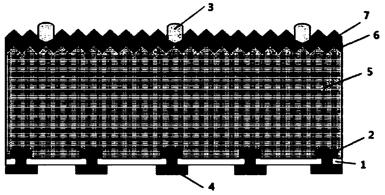
[0056] S1: Select 156×156mm P-type silicon, form a textured surface on the front side of the silicon wafer, use wet or dry etching technology to form a textured surface on the surface of the P-type silicon wafer, and control the reflectivity at 20%.

[0057] S2: Phosphorus is diffused on the front side of the silicon wafer treated in S1 to form an N-type emitter. The N-type emitter can be formed by thermal diffusion or ion implantation, wherein the diffusion of the silicon wafer is preferably made of phosphorus oxychloride , it is necessary to control the sheet resistance at 90ohm / sq during diffusion.

[0058] S3: On the basis of S2, the device removes the phosphosilicate glass formed during the diffusion process, and uses HF solution to remove the phosphosilicate glass layer formed during the diffusion process on the front of the N-type emitter and the back of the P-type silicon wafer...

Embodiment 2

[0065] S1: Select 156×156mm P-type silicon, form a textured surface on the front side of the silicon wafer, use wet or dry etching technology to form a textured surface on the surface of the P-type silicon wafer, and control the reflectivity at 10%.

[0066] S2: Phosphorus is diffused on the front side of the silicon wafer treated in S1 to form an N-type emitter. The N-type emitter can be formed by thermal diffusion or ion implantation, wherein the diffusion of the silicon wafer is preferably made of phosphorus oxychloride , it is necessary to control the sheet resistance at 75ohm / sq during diffusion.

[0067] S3: On the basis of S2, the device removes the phosphosilicate glass formed during the diffusion process, and uses HF solution to remove the phosphosilicate glass layer formed during the diffusion process on the front of the N-type emitter and the back of the P-type silicon wafer.

[0068] S4: Use PVECD equipment to first deposit 8nm aluminum oxide or silicon dioxide on ...

Embodiment 3

[0074] S1: Select 156×156mm P-type silicon, form a textured surface on the front side of the silicon wafer, use wet or dry etching technology to form a textured surface on the surface of the P-type silicon wafer, and control the reflectivity at 30%.

[0075] S2: Phosphorus is diffused on the front side of the silicon wafer treated in S1 to form an N-type emitter. The N-type emitter can be formed by thermal diffusion or ion implantation, wherein the diffusion of the silicon wafer is preferably made of phosphorus oxychloride , it is necessary to control the sheet resistance at 75ohm / sq during diffusion.

[0076] S3: On the basis of S2, the device removes the phosphosilicate glass formed during the diffusion process, and uses HF solution to remove the phosphosilicate glass layer formed during the diffusion process on the front of the N-type emitter and the back of the P-type silicon wafer.

[0077] S4: Use PVECD equipment to first deposit 8nm aluminum oxide or silicon dioxide on ...


PUM


Abstract

The invention discloses a double-sided power generation solar cell. The double-sided power generation solar cell comprises a silicon substrate, and an N emitting electrode, a front antireflection passivation film and a front electrode which are sequentially arranged on the front surface of the silicon substrate from bottom to top, and a back passivation film, a back electric field and a back electrode which are arranged on the back surface of the silicon substrate from top to bottom; the solar cell is a double-sided solar cell; the back electric field is a local aluminum back electric field; through the local aluminum back electric field, a linear open groove is formed after the back passivation film is etched by inorganic etching paste, and then the open groove is covered by high-conductivity aluminum paste; and the solar cell is provided with a BSF layer with the thickness of 2-5 microns. According to the back electric field structure of the solar cell, the thickness of the BSF layercan be increased, the destruction of the silicon substrate is reduced, the aluminum paste consumption is reduced, and therefore the photoelectric conversion rate is improved.

Description

technical field [0001] The invention belongs to the technical field of photovoltaics, and in particular relates to a double-sided power generating solar cell and a preparation method thereof. Background technique [0002] Photovoltaic technology is a technology that uses large-area p-n junction diodes to convert solar energy into electrical energy. This p-n junction diode is called a solar cell. The semiconductor materials used to make solar cells have a certain band gap. When the solar cell is irradiated by the sun, photons with energy exceeding the band gap generate electron-hole pairs in the solar cell. The p-n junction separates the electron-hole pairs, and the p-n junction The asymmetry determines the flow direction of different types of photo-generated carriers, and the external power can be output through the external circuit connection. This is similar to the principle of ordinary electrochemical cells. [0003] Industrial production of p-type crystalline silicon ...

Claims


Application Information

Patent Timeline
Patent Type & Authority Applications(China)
IPC IPC(8): H01L31/0216H01L31/0224H01L31/068H01L31/18
CPCH01L31/02168H01L31/022425H01L31/0684H01L31/1804Y02E10/547H01L31/068H01L31/02167
Inventor 朱鹏刘媛吴广郑金华
Owner NANTONG T SUN NEW ENERGY CO LTD
Why Eureka
Try Eureka