Ceramic sensitive core based on high temperature co-sintering and preparation method thereof
A technology of co-sintering and ceramics, which is applied in the field of high-temperature sensors, can solve the problems that the preparation process cannot meet the requirements of the ultra-high temperature measurement environment and the sensor has low precision, and achieve the effects of reducing the overall size, uniform temperature, and good thermal conductivity
- Summary
- Abstract
- Description
- Claims
- Application Information
AI Technical Summary
Problems solved by technology
Method used
Image
Examples
specific Embodiment approach 1
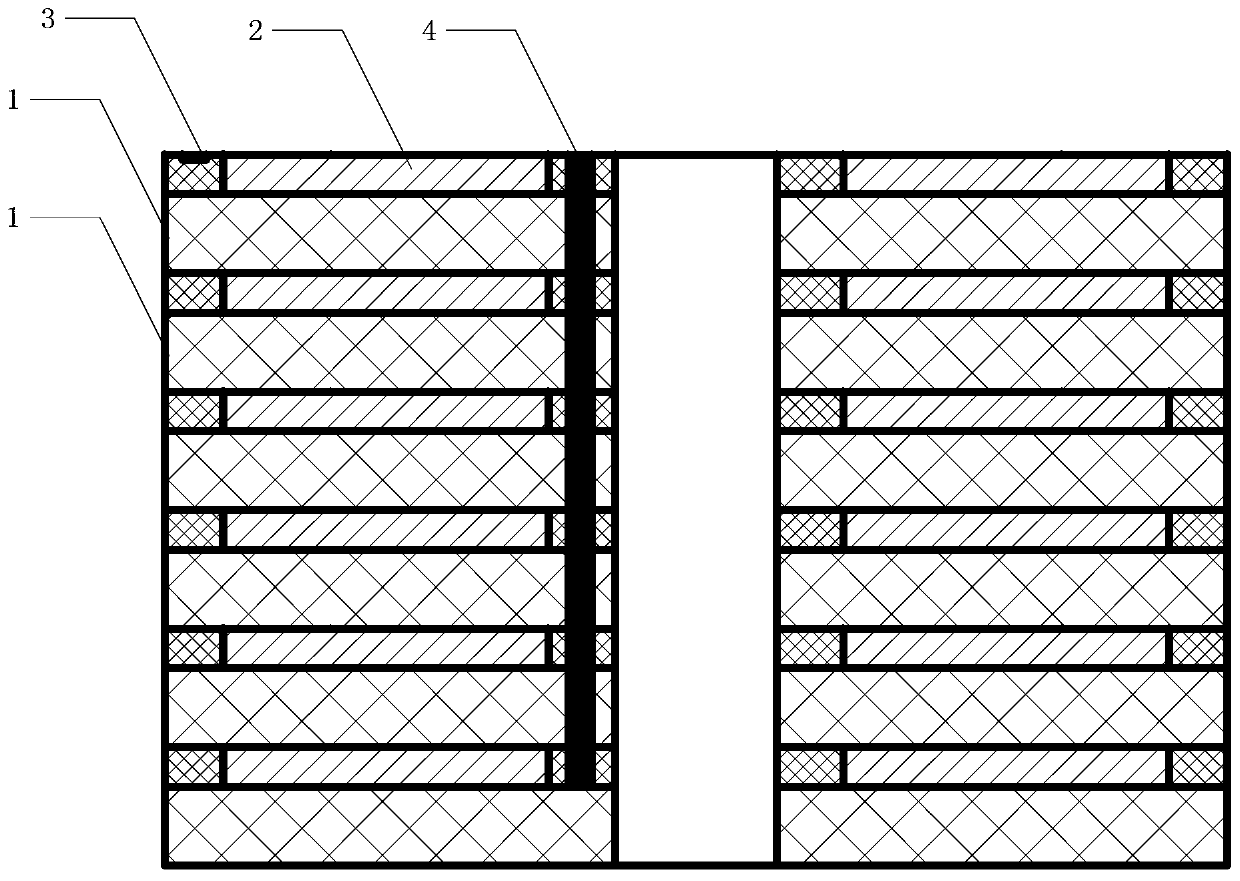
[0035] Specific implementation mode one: the following combination Figure 1-Figure 5 Describe this embodiment, the ceramic sensitive core body based on high-temperature co-sintering described in this embodiment, N-layer functional layer substrates are co-sintered at high temperature to form a ceramic sensitive core body, N is a positive integer greater than or equal to 2;
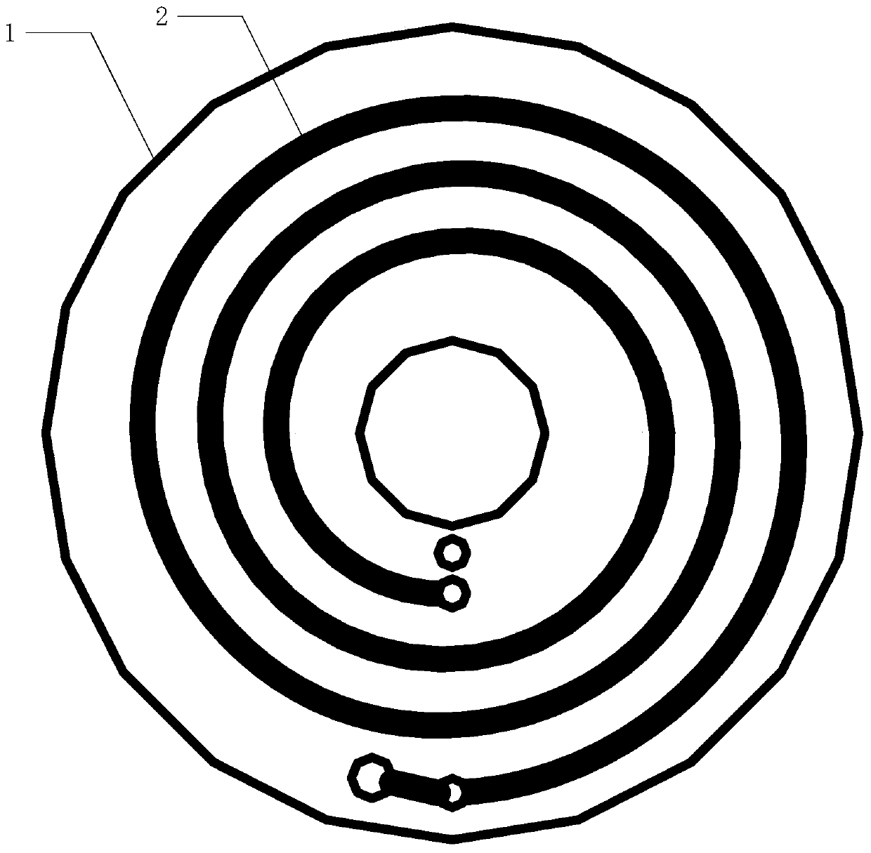
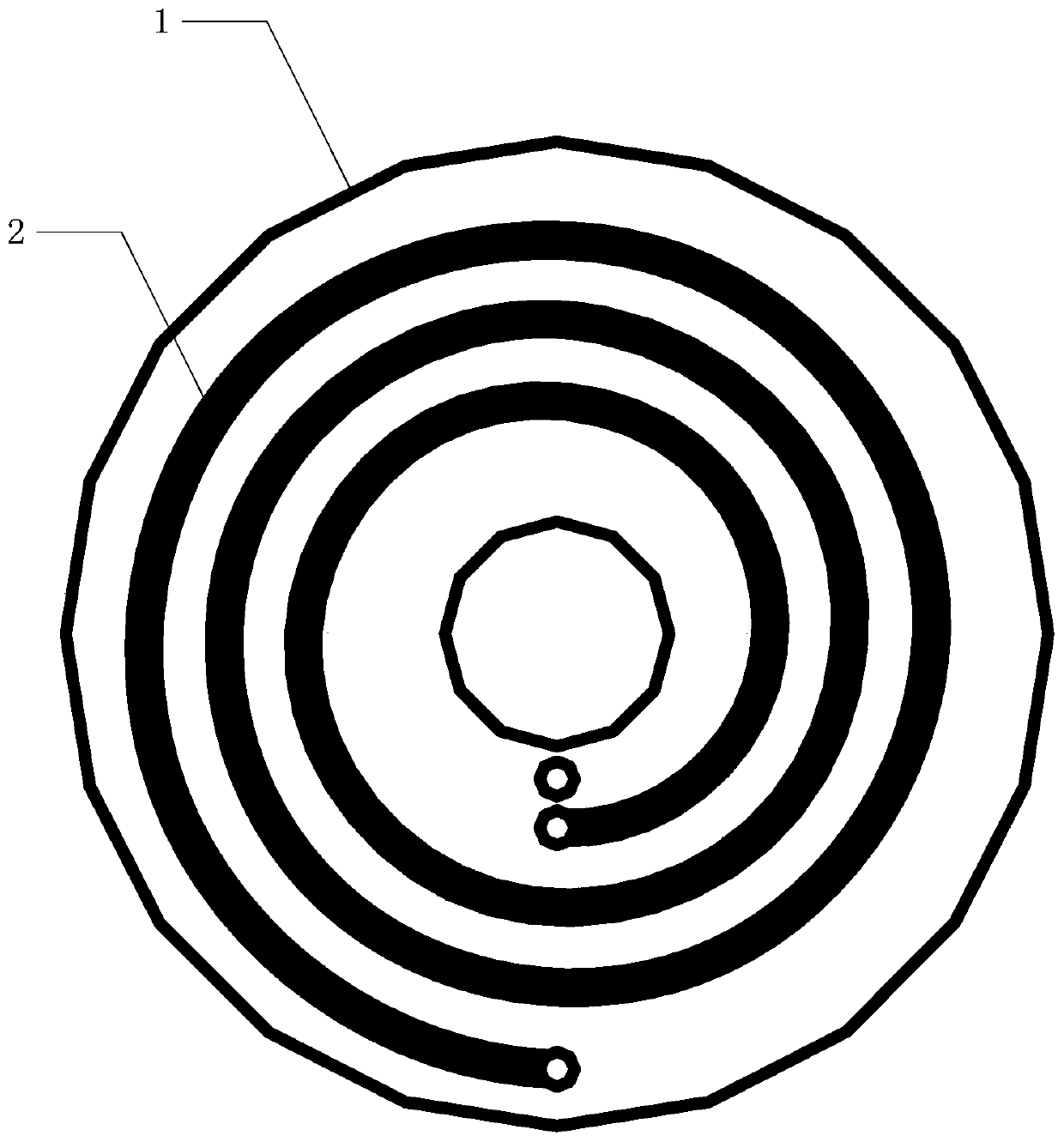
[0036] The functional layer substrate includes a ceramic substrate 1, a spiral coil 2, a filled ceramic 3 and a signal lead-out hole 4;
[0037] The ceramic substrate 1 is circular, and the spiral coil 2 is spirally printed on the ceramic substrate 1, and the blank of the ceramic substrate 1 is overprinted with filled ceramics 3;
[0038] The helical coils 2 on adjacent functional layer substrates have opposite directions of rotation.
[0039] In this embodiment, the signal lead-out hole 4 is a through hole for realizing electrical connection.
[0040] In this embodiment, the helical coils 2 on adjacent ...
specific Embodiment approach 2
[0045] Specific embodiment two: the preparation method of the ceramic sensitive core based on high temperature co-sintering described in this embodiment, the specific process of the preparation method is:
[0046] S1. Prepare a cast film according to the set shrinkage rate and thermal expansion coefficient;
[0047] S2. Cut the casting film into ceramic substrate 1 according to the set size;
[0048] S3, punch out the signal lead-out hole 4 on the ceramic substrate 1;
[0049] S4, using metal paste to screen-print the spiral coil 2 on the ceramic substrate 1; at the same time, metallize the signal lead-out hole 4 obtained in S3;
[0050] S5. Prepare the filled ceramic 3, and overprint the filled ceramic 3 on the blank space of the ceramic substrate 1, and the preparation of the functional layer substrate is completed;
[0051] S6. Laminating the prepared functional layer substrates together, and cutting the helical coils 2 of adjacent functional layer substrates in the oppos...
PUM
 Abstract
Description
Claims
Application Information
 - R&D
- Intellectual Property
- Life Sciences
- Materials
- Tech Scout
- Unparalleled Data Quality
- Higher Quality Content
- 60% Fewer Hallucinations
Browse by: Latest US Patents, China's latest patents, Technical Efficacy Thesaurus, Application Domain, Technology Topic, Popular Technical Reports.
© 2025 PatSnap. All rights reserved.Legal|Privacy policy|Modern Slavery Act Transparency Statement|Sitemap|About US| Contact US: help@patsnap.com


