Method for preparing sample observing orientation of crystal grains in Al metallization layer of IGBT chip

A sample preparation and metallization technology, which is applied in the preparation of test samples, material analysis by wave/particle radiation, sampling, etc., can solve the problem that the Al metallization layer cannot be observed, the Al metallization layer becomes rough, and cannot be obtained. Problems such as poor crystal orientation

Active Publication Date: 2019-10-01
BEIJING UNIV OF TECH
View PDF3 Cites 4 Cited by
  • Summary
  • Abstract
  • Description
  • Claims
  • Application Information

AI Technical Summary

Problems solved by technology

[0002] At present, after completing the power cycle test or temperature cycle test of the high-power IGBT module, in order to observe the crystal orientation of the crystal grains in the Al metallization layer of the high-power IGBT chip subjected to different cycles, the current method is to use X-ray diffraction (XRD, X-ray diffraction) is used to test the crystal orientation of the Al metallization layer of the high-power IGBT chip. Compared with the EBSD technology, the XRD technology cannot obtain the crystal orientation of each grain and the orientation difference between the grains
As the power cycle test or temperature cycle test proceeds, the Al metallization layer gradually becomes rough, so it is impossible to observe the Al metallization layer on the surface of the high-power IGBT chip after the cycle test by EBSD technology

Method used


Image

  • Method for preparing sample observing orientation of crystal grains in Al metallization layer of IGBT chip
  • Method for preparing sample observing orientation of crystal grains in Al metallization layer of IGBT chip
  • Method for preparing sample observing orientation of crystal grains in Al metallization layer of IGBT chip

Examples


Embodiment

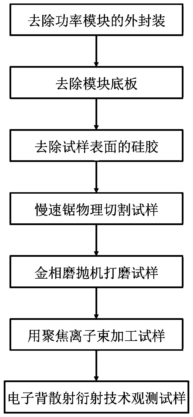
[0034] A method for preparing a sample for observing the grain direction in the Al metallization of an IGBT chip, characterized in that it comprises the following steps:

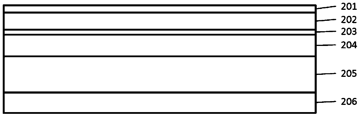
[0035] A) Remove the outer package of the high-power IGBT module by machining;

[0036] B) Set the temperature of the constant-temperature heating platform to 250°C, place the high-power IGBT module on the constant-temperature heating platform, and keep the bottom plate of the power module in contact with the constant-temperature heating platform for about 30 seconds, until the solder layer between the copper-clad ceramic substrate and the bottom plate is melted, Remove the bottom plate of the module, and the module structure at this time only leaves the high-power IGBT chip layer and the copper-clad ceramic substrate;

[0037] C) soaking the remaining structure of the high-power IGBT module in step B) in a silica gel remover for 12 hours to remove the silica gel on the surface of the IGBT chip;
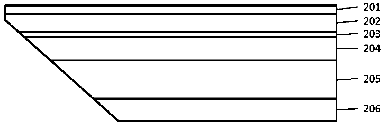
[0038] D)...


PUM

PropertyMeasurementUnit
lengthaaaaaaaaaa
widthaaaaaaaaaa
heightaaaaaaaaaa

Abstract

The invention discloses a method for preparing a sample observing orientation of crystal grains in an Al metallization layer of an IGBT chip. The method comprises following steps of: removing outer packaging of a high power IGBT module; removing a module bottom plate; removing silica gel on the surface of the sample; cutting the sample by using a low-speed saw in a physical manner; polishing the sample by using a metallographic grinding and polishing machine; processing the sample by using a focused ion beam; and observing the sample by using an electron back-scattered diffraction technology.The preparation method has the advantage of preparing the sample observing orientation of crystal grains on a cross section of an Al metallization layer of the high power IGBT chip, is simple and feasible, can observe orientation of crystal grains on the cross section of the Al metallization layer of the high power IGBT chip.

Description

technical field [0001] The invention relates to the observation technology of the microstructure of materials, in particular to a sample preparation method for observing the grain direction of the Al metallization in the IGBT chip. Background technique [0002] At present, after completing the power cycle test or temperature cycle test of the high-power IGBT module, in order to observe the crystal orientation of the crystal grains in the Al metallization layer of the high-power IGBT chip subjected to different cycles, the current method is to use X-ray diffraction (XRD, X-ray diffraction) The crystal orientation test is performed on the Al metallization layer of the high-power IGBT chip. Compared with the EBSD technology, the XRD technology cannot obtain the crystal orientation of each crystal grain and the orientation difference between crystal grains. As the power cycle experiment or temperature cycle experiment proceeds, the Al metallization layer gradually becomes rough,...

Claims


Application Information

Patent Timeline
Patent Type & Authority Applications(China)
IPC IPC(8): G01N23/2202G01N23/2251G01N1/32G01N1/28
CPCG01N23/2202G01N23/2251G01N1/32G01N1/286G01N2001/2866
Inventor 安彤袁雪泉秦飞别晓锐赵静毅方超
Owner BEIJING UNIV OF TECH
Why Eureka
Try Eureka