Composite-structure dual-absorption layer graphene detector and fabrication process thereof
A double-absorbing layer, composite structure technology, applied in sustainable manufacturing/processing, semiconductor device, final product manufacturing, etc. Photoelectric responsivity, high reliability, and strong practicability
- Summary
- Abstract
- Description
- Claims
- Application Information
AI Technical Summary
Problems solved by technology
Method used
Image
Examples
Embodiment Construction
[0028] In order to make the objectives, technical solutions, and advantages of the present invention clearer, the principle and experimental process of the present invention will be further explained below with reference to the accompanying drawings.
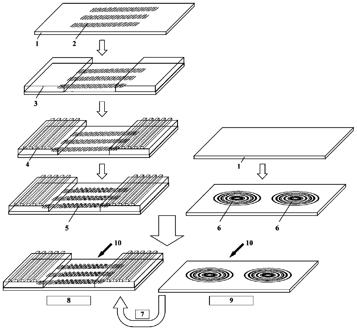
[0029] Such as figure 1 As shown, the present invention provides a composite structure double absorption layer graphene detector, including a silica substrate 1, graphene nanoribbons 2, metal electrodes 3, nano grating antenna 4, metal quantum dots 5, metal film ring belt Sheet 6 and transparent adhesive 7. Among them, the silicon dioxide substrate 1, the graphene nanoribbons 2, the metal electrode 3, the nano-grating antenna 4, and the metal quantum dots 5 constitute the front face 8 of the detector; the silicon dioxide substrate 1, the metal film ring belt sheet 6 constitute the detector Back 9. The front side 8 of the detector and the back side 9 of the detector are organically combined by a transparent adhesive 7 to form a gr...
PUM
 Abstract
Description
Claims
Application Information
 - R&D
- Intellectual Property
- Life Sciences
- Materials
- Tech Scout
- Unparalleled Data Quality
- Higher Quality Content
- 60% Fewer Hallucinations
Browse by: Latest US Patents, China's latest patents, Technical Efficacy Thesaurus, Application Domain, Technology Topic, Popular Technical Reports.
© 2025 PatSnap. All rights reserved.Legal|Privacy policy|Modern Slavery Act Transparency Statement|Sitemap|About US| Contact US: help@patsnap.com

