Resin hole plugging method for manufacturing 5G circuit board

A technology for circuit board manufacturing and resin plugging, which is used in printed circuit manufacturing, printed circuits, printed circuits, etc., can solve problems such as holes that cannot be filled, air bubbles in holes, and affect physical health, and achieves cost saving and volatilization reduction. Effect

Inactive Publication Date: 2019-09-06
AOSHIKANG TECH CO LTD
View PDF9 Cites 4 Cited by
  • Summary
  • Abstract
  • Description
  • Claims
  • Application Information

AI Technical Summary

Problems solved by technology

[0003] 1. Due to the bottleneck factor of the aspect ratio of the thick plate and small hole type circuit board, the holes cannot be filled, resulting in quality defects such as air bubbles in the holes, orifice depressions;
[0004] 2. The existing plugging process uses expensive ink resin and high production cost;
[0005] 3. The existing plugging process needs to be baked, and the harmful gas will be volatilized and affect the health

Method used


Image

  • Resin hole plugging method for manufacturing 5G circuit board
  • Resin hole plugging method for manufacturing 5G circuit board

Examples


Embodiment 1

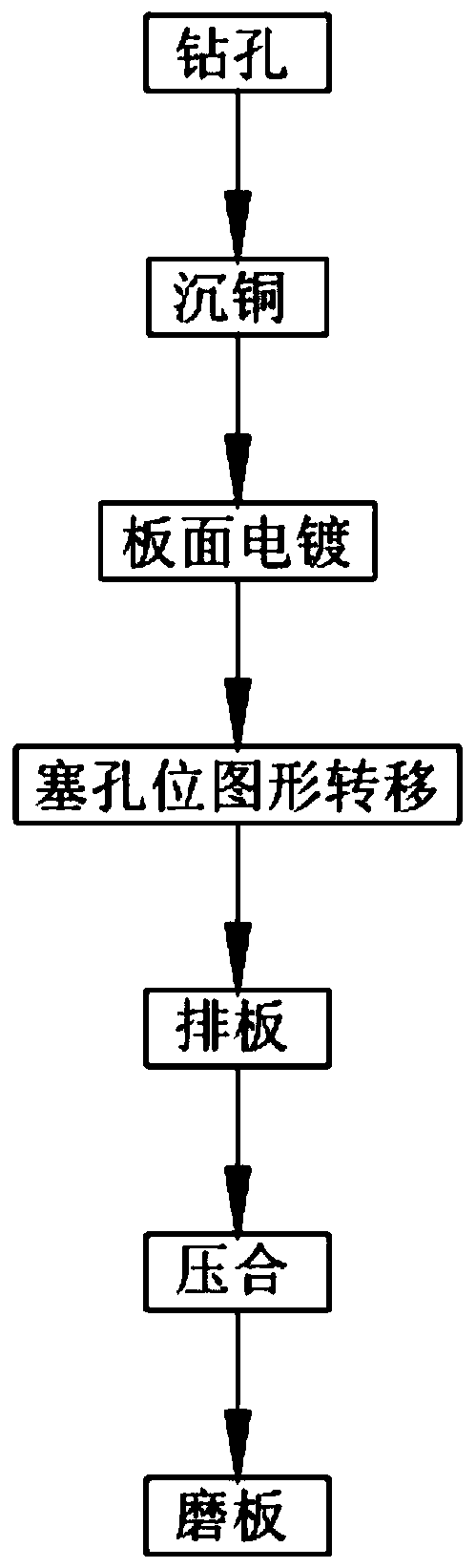
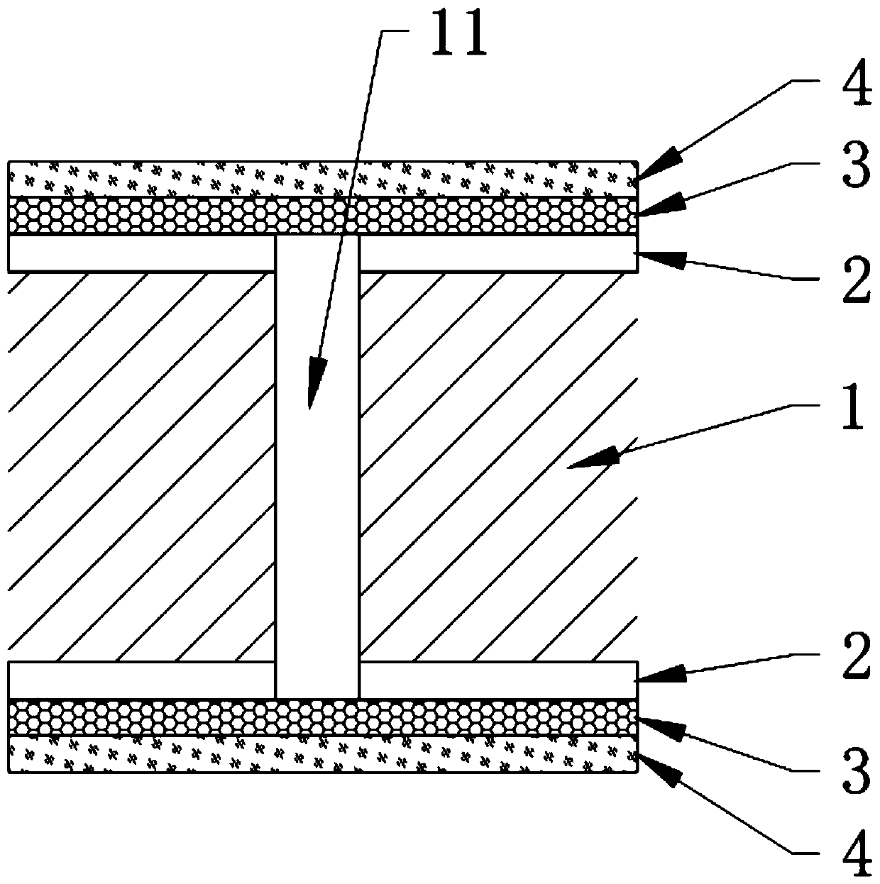
[0032] Please also refer to figure 1 and figure 2 , this embodiment includes the following steps:

[0033] Drilling: Drill holes on a circuit board with a thickness of 4mm and an aspect ratio of 20:1;

[0034] Copper sinking: decontaminate the circuit board first, then put the decontaminated circuit board into the copper sinking potion, and conduct preliminary copper sinking on the surface of the circuit board and the wall of the hole;

[0035] Board surface electroplating: the whole board is electroplated to obtain a conductive copper layer with a set thickness;

[0036] Plug hole pattern transfer: paste photosensitive film on both sides of the circuit board, the temperature resistance of the photosensitive film is 200°C, the speed of photosensitive film is 0.5m / min, and the film pressure is 1kg / cm 2 , the temperature of the film is 120°C, and then the circuit board covered by the photosensitive film is exposed and developed. 2 , The developing temperature is 35°C, wash ...

Embodiment 2

[0041] Please also refer to figure 1 and figure 2 , this embodiment includes the following steps:

[0042] Drilling: Drill holes on a circuit board with a thickness of 5mm and an aspect ratio of 25:1;

[0043] Copper sinking: decontaminate the circuit board first, then put the decontaminated circuit board into the copper sinking potion, and conduct preliminary copper sinking on the surface of the circuit board and the wall of the hole;

[0044] Board surface electroplating: the whole board is electroplated to obtain a conductive copper layer with a set thickness;

[0045] Plug hole pattern transfer: stick a photosensitive film on both sides of the circuit board, the temperature resistance of the photosensitive film is 200°C, the film sticking speed of the photosensitive film is 0.5m / min, and the film sticking pressure is 2kg / cm 2 , the temperature of the film is 130°C, and then the circuit board covered by the photosensitive film is exposed and developed. 2 , The developi...


PUM


Abstract

The invention provides a resin hole plugging method for manufacturing a 5G circuit board. The resin hole plugging method comprises the steps: hole drilling; copper plating; board surface electroplating; plug hole position pattern transferring: photosensitive films are pasted on the two surfaces of a circuit board, then the circuit board covered by the photosensitive films is exposed and developedand the photosensitive film covering the plug hole is punched in the punching porcess; board layout: PP resin is used for covering the two surfaces of the circuit board and then a release film is usedfor covering the PP resin; press-bonding: the laminated circuit board, PP resin and release film are press-bonded by a vacuum pressing machine, and the PP resin is heated and molten and penetrates into the hole under the action of the mechanical pressure and cooled and solidified; and board grinding: the release film, the PP resin and the photosensitive films are stripped and partial residual PPresin is removed by an abrasive belt grinding plate. The resin hole plugging method for manufacturing the 5G circuit board has high hole plugging quality, low production cost, health and environmentalprotection.

Description

technical field [0001] The invention relates to the technical field of circuit board processing, in particular to a resin plugging method for manufacturing 5G circuit boards. Background technique [0002] With the continuous development of my country's mobile communication industry, it has developed to the fifth generation mobile communication system (5G). Technical requirements such as large data traffic, high speed, and low latency of 5G communication have become the norm. Therefore, there are higher requirements for circuit boards. In the circuit board resin plugging process, after the circuit board is drilled and plated, the hole needs to be filled and filled with resin. The existing plugging technology has the following problems; [0003] 1. Due to the bottleneck factor of the aspect ratio of the thick plate and small hole type circuit board, the hole cannot be filled, resulting in quality defects such as air bubbles in the hole, orifice depression; [0004] 2. The ex...

Claims


Application Information

Patent Timeline
Patent Type & Authority Applications(China)
IPC IPC(8): H05K3/00H05K3/42
CPCH05K3/0094H05K3/42H05K2201/0959
Inventor 杨先卫
Owner AOSHIKANG TECH CO LTD
Why Eureka
Try Eureka