A widely distributed low-jitter synchronous clock distribution system and method
A technology for synchronizing clocks and distribution systems, applied in automatic power control, electrical components, etc., can solve problems such as large time jitter of optical modules and impact on system stability, and achieve an efficient and concise solution
- Summary
- Abstract
- Description
- Claims
- Application Information
AI Technical Summary
Problems solved by technology
Method used
Image
Examples
Embodiment 1
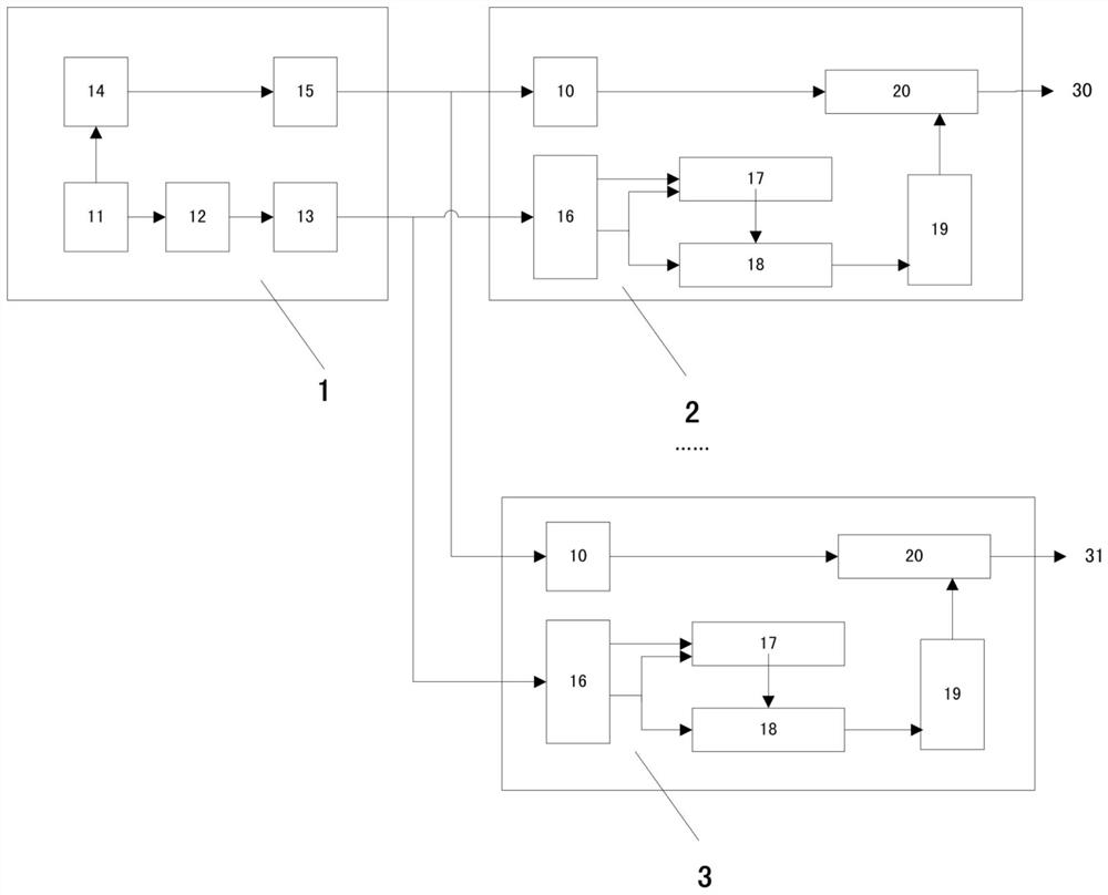
[0045] Embodiment 1 of the present invention provides a widely distributed low-jitter synchronous clock distribution system. The system is mainly composed of a precise timing generation component and a phase-locked clock generator. The precision timing generating component generates a high-frequency clock optical data stream and a low-frequency clock and reset code mixed-encoded optical data stream. The phase-locked clock generator recovers the low-frequency clock and the reset start signal through the clock and data recovery module. The reset code is extracted from the recovered data under the action of the recovered clock, and a reset pulse signal is generated under the action of the recovered clock. The micro-step delay module provides a cycle center reset pulse signal by performing a micro-step delay on the reset pulse signal. The phase-locked clock generator uses clock recovery technology to recover a low-jitter high-frequency clock signal from the high-frequency clock op...
Embodiment 2
[0056] This embodiment provides a method for providing widely distributed low-jitter synchronous clock distribution, and the method is implemented based on any of the aforementioned widely distributed low-jitter synchronous clock distribution systems. The method comprises the steps of:
[0057] Step S1, initialization, generating and outputting a reference clock by an external reference clock source 11;
[0058] Step S2, process and convert the reference clock output by the external reference clock source 11, so as to simultaneously generate low-frequency clock and high-frequency clock, and transmit them in the form of two optical data streams;
[0059] Further, step S2 specifically includes:
[0060] Step S2.1, the reference clock output by the external reference clock source 11 is a low-frequency clock signal, and the low-frequency clock signal is simultaneously provided as an input to the clock and reset signal encoding module 12 and the phase-locked frequency multiplier 1...
Embodiment 3
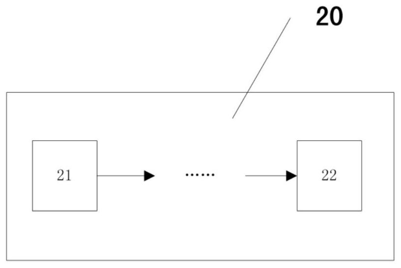
[0076] It is necessary to perform a micro-step delay on the reset pulse signal generated by the micro-step delay module 19 in the foregoing embodiment, move the reset pulse signal to the center of the clock cycle, and output a low-jitter reset solution. In the frequency divider, the frequency division state of the frequency divider is in an uncertain state when it is turned on, which will cause the output of the frequency divider to be in an uncertain state, and the jitter is large. In order to ensure the low jitter output of the frequency It is necessary to reset the frequency divider once every time, and fix the output state of the frequency divider. The frequency divider operates at the edge of the high-frequency clock, and when the reset signal is at the edge of the high-frequency clock, the clock frequency division output will be in an indeterminate state, that is, the output clock has periodic jitter. The position of the reset signal can be adjusted by the micro-step del...
PUM
 Abstract
Description
Claims
Application Information
 - R&D
- Intellectual Property
- Life Sciences
- Materials
- Tech Scout
- Unparalleled Data Quality
- Higher Quality Content
- 60% Fewer Hallucinations
Browse by: Latest US Patents, China's latest patents, Technical Efficacy Thesaurus, Application Domain, Technology Topic, Popular Technical Reports.
© 2025 PatSnap. All rights reserved.Legal|Privacy policy|Modern Slavery Act Transparency Statement|Sitemap|About US| Contact US: help@patsnap.com


