Avalanche photodiode and manufacturing method thereof

An avalanche optoelectronics and manufacturing method technology, which is applied in the direction of circuits, electrical components, semiconductor devices, etc., can solve the problems of increased manufacturing cost of diodes, decreased device yield, and reduced device consistency, so as to suppress pre-breakdown and reduce edge Curvature, the effect of improving device performance

Pending Publication Date: 2019-08-30
武汉光谷量子技术有限公司
View PDF0 Cites 2 Cited by
  • Summary
  • Abstract
  • Description
  • Claims
  • Application Information

AI Technical Summary

Problems solved by technology

Although the above two methods can suppress edge breakdown, due to the complex process and difficult control, it is easy to cause problems such as increased diode manufacturing costs, reduced device yield, and reduced device consistency.

Method used


Image

  • Avalanche photodiode and manufacturing method thereof
  • Avalanche photodiode and manufacturing method thereof
  • Avalanche photodiode and manufacturing method thereof

Examples


Embodiment Construction

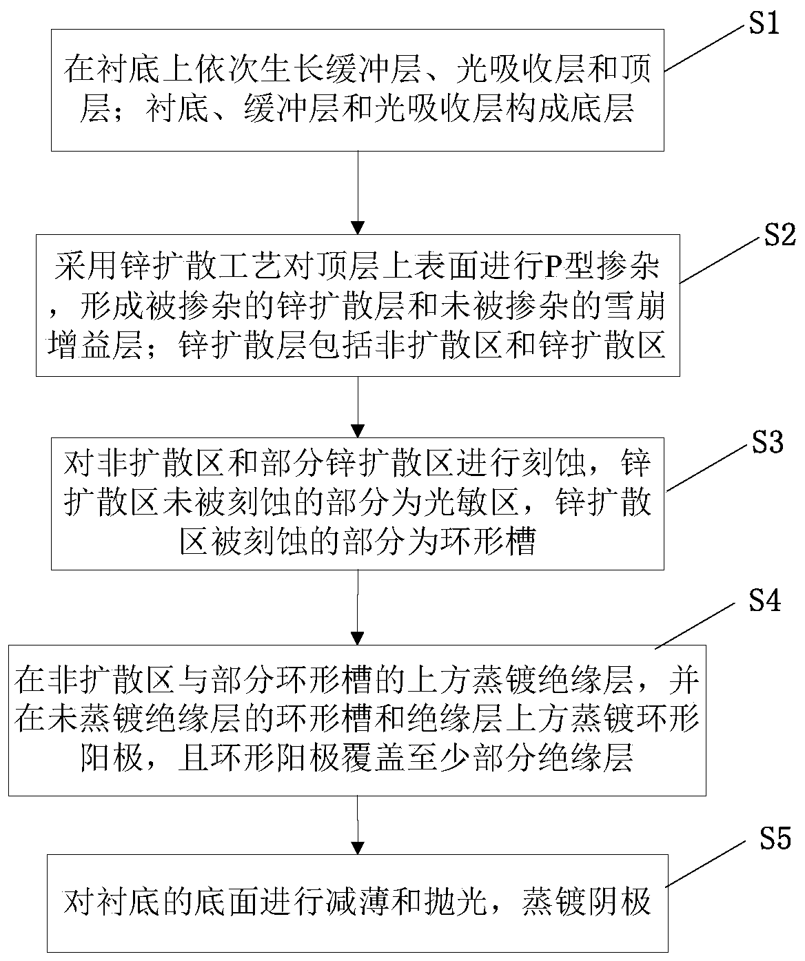
[0042] The present invention will be described in further detail below in conjunction with the accompanying drawings and embodiments.

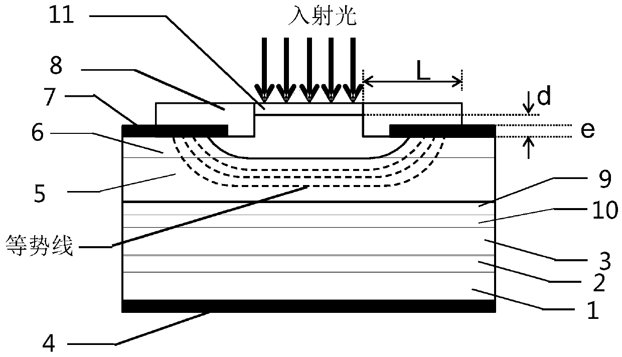
[0043] see figure 1 As shown, the embodiment of the present invention provides an avalanche photodiode, which includes a bottom layer and a top layer. A cathode 4 made of semiconductor material is also provided. In this embodiment, the substrate 1 is made of InP material, the buffer layer 2 is made of n-type low-doped InP material, and the light absorbing layer 3 is made of intrinsic InGaAs material.

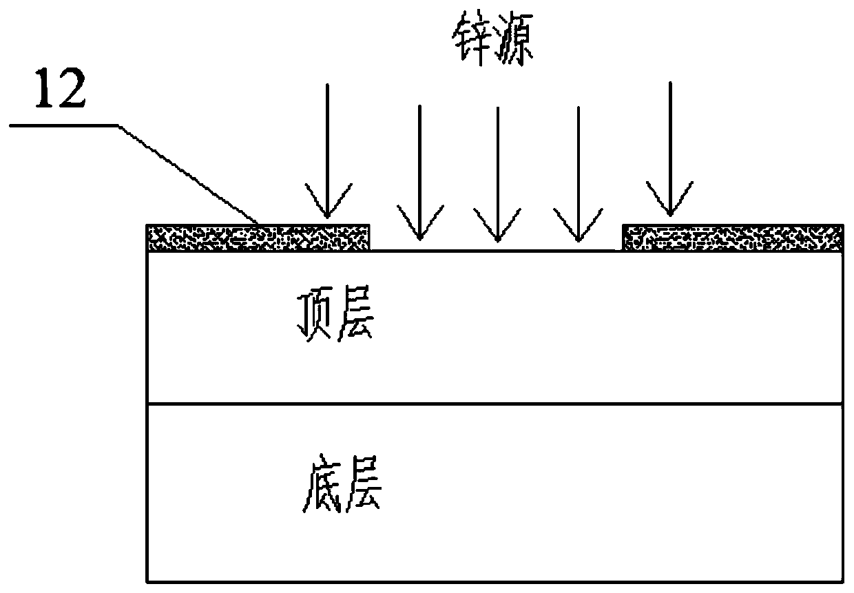
[0044] The top layer is arranged above the bottom layer, ie above the light absorbing layer 3 . Since the diffusion rate of zinc in the InP material is relatively high, it is easier to obtain a deeper diffusion morphology. Therefore, the top layer is made of n-type low doping or intrinsic InP material. The top layer includes an avalanche gain layer 5 and a zinc diffusion layer 6 disposed above the avalanche gain layer 5 , that is, the undoped...


PUM


Abstract

The invention discloses an avalanche photodiode and a manufacturing method thereof, and relates to the technical field of photodiodes. The avalanche photodiode comprises a bottom layer and a top layer, wherein the bottom layer includes a substrate, a buffer layer and a light absorption layer, and the lower surface of the substrate is provided with a cathode; the top layer is arranged above the bottom layer and includes an avalanche gain layer and a zinc diffusion layer; the zinc diffusion layer includes a non-diffusion region and a zinc diffusion region, the non-diffusion region and part of the zinc diffusion region are etched, the part, which is not etched, of the zinc diffusion region is a photosensitive region, and the etched part of the zinc diffusion region is an annular groove; an insulating layer is evaporated on the non-diffusion region and part of the annular groove, and an annular anode is evaporated on the annular groove which is not evaporated with the insulating layer andthe insulating layer; and the annular anode, the insulating layer and the cathode form an MIS structure. The avalanche photodiode of the invention can generate an anode capacitance effect, change theelectric field distribution at the edge of a p-type doping region below the anode, reduces the curvature at the edge of a depletion region, reduce the edge electric field intensity and thus suppress the edge pre-breakdown.

Description

technical field [0001] The invention relates to the technical field of photodiodes, in particular to an avalanche photodiode and a manufacturing method thereof. Background technique [0002] When manufacturing planar avalanche photodiodes (Avalanche Photodiodes: APD), especially APDs based on III-V materials, the size of the photosensitive surface of the device is determined by the zinc diffusion window, and the edge area of ​​the diffusion window is caused by the curvature effect. The electric field intensity in the area is higher than that in the central area of ​​the photosensitive surface, resulting in a lower gain in the central part of the photosensitive surface of the device, that is, the gain available in practical applications is lower, and edge pre-breakdown is prone to occur, making it impossible to use normally. [0003] The existing APD methods for suppressing edge pre-breakdown mainly include: 1. Perform epitaxial regrowth after etching the area around the char...

Claims


Application Information

Patent Timeline
IPC IPC(8): H01L31/107H01L31/0352H01L31/18
CPCH01L31/1075H01L31/035272H01L31/1844Y02P70/50
Inventor 曾磊王肇中李永平
Owner 武汉光谷量子技术有限公司
Why Eureka
Try Eureka