Integrated measuring device for surface dielectric properties of solid insulating materials

A technology of solid insulating materials and dielectric properties, applied in measuring devices, measuring electrical variables, measuring resistance/reactance/impedance, etc., can solve the problem that the secondary electron emission characteristics of materials cannot be measured, and the surface of insulating materials cannot be truly and comprehensively reflected Dielectric properties, inability to measure secondary electron emission characteristics of materials, etc.

Inactive Publication Date: 2019-08-23
INST OF ELECTRICAL ENG CHINESE ACAD OF SCI
View PDF8 Cites 6 Cited by
  • Summary
  • Abstract
  • Description
  • Claims
  • Application Information

AI Technical Summary

Problems solved by technology

The current devices measure one of the three parameters separately, and the measurement environment and measurement conditions are different, so there is a problem that the experimental data cannot be compared
At the same time, the measurement of a single parameter cannot truly and comprehensively reflect the dielectric properties of the insulating material surface, and can only reflect a specific process one-sidedly.
At present, most of the devices for measuring charge traps inject charges into the sample through corona, which can only measure the charge trap parameters on the surface of the material, but cannot measure the trap parameters at a certain depth.
[0003] The Chinese patent No. 201410022709.1 discloses a secondary electron emission coefficient measurement device based on a hemispherical collector structure. The device distinguishes true secondary electrons from backscattered electrons through a multi-layer spherical mesh screen, and passes through a pulsed electron beam. To reduce the impact of dielectric material surface charge on secondary electron emission, the device mainly measures the secondary electron emission characteristics of materials in a vacuum environment, and cannot measure the surface charge and trap parameter distribution of materials
The Chinese patent with the patent number 201410023001.8 discloses a measuring device for the secondary electron emission coefficient of the flat plate collector. The device provides a rotating sample stage, and the sample is rotated at a certain angle before and after each measurement to avoid multiple measurements at the same position. In order to reduce the influence of the surface charge of the insulating material on the secondary electron emission coefficient, but there is a large gap between the collector and the sample, so it is difficult to guarantee the secondary electron collection efficiency; the Chinese patent No. 201010617890.2 discloses A test device for distinguishing secondary electrons from backscattered electrons. The device discloses a hemispherical collection structure composed of collectors and retardation grids. By applying different voltages to the retardation grids, the secondary electrons and backscattered The distinction of scattered electrons and the energy spectrum analysis of secondary electrons, but this device can only be used for the measurement of metal materials, and the accumulation of material surface charges will seriously affect the measurement results when measuring insulating materials; these two devices can only measure the secondary of materials Sub-electronic properties, unable to measure the surface charge and trap parameter distribution of the material
[0004] The Chinese patent No. 2009100231880 discloses an automatic measurement device for the surface charge distribution of a solid medium. The device uses an electrostatic probe to measure the surface charge of insulating materials, and can measure the two-dimensional charge distribution through a two-dimensional motion platform, but the device only Can measure surface charge in a fixed environment and cannot measure secondary electron emission properties of materials
[0005] The Chinese patent No. 2014104587908 discloses a solid dielectric material trap parameter acquisition system. The device uses three-electrode corona charging to inject charges into the sample, heats the sample through the heating system, and the electrostatic probe measures the surface charge decay. According to the surface Calculate the trap parameters of the sample based on the charge decay. The device can only measure the charge traps on the surface of the material, but cannot measure the trap parameters at a certain depth; at the same time, the device cannot measure the secondary electron emission characteristics of the material

Method used


Image

  • Integrated measuring device for surface dielectric properties of solid insulating materials
  • Integrated measuring device for surface dielectric properties of solid insulating materials

Examples


Embodiment 1

[0044] Secondary electron emission coefficient, surface charge and charge trap measurement steps in high vacuum environment:

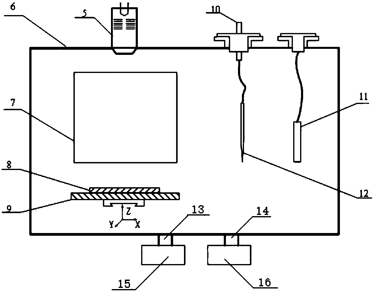
[0045] 1) Place the sample 8 on the sample stage 9, set the temperature of the sample stage 9, evacuate the external cavity 6, and heat the sample 8 to the specified temperature.

[0046] 2) Move the sample stage 9 to below the collector 7, set the electron beam energy and beam current I of the electron gun 5 P , the electron beam bombards the surface of the material, and the secondary electron collector 7 collects the secondary current I SE , according to the secondary electron emission coefficient σ=I SE / I P Calculate the secondary electron emission coefficient.

[0047] 3) Using the electron gun 5 to charge the sample.

[0048] 4) After charging is completed, move the sample stage 9 to the bottom of the electrostatic probe 11 of the surface potential measurement module 4, measure the distribution of the surface potential of the sample 8, and ob...

Embodiment 2

[0051] Surface potential and charge trap measurement steps in high pressure environment:

[0052] 1) First place the sample 8 on the sample stage 9, set the temperature of the sample stage 9, and heat the sample 8 to the specified temperature.

[0053] 2) The sample stage 9 is moved to the bottom of the corona needle 12, and the outer cavity 6 is evacuated and filled with working gas to a certain pressure.

[0054] 3) Applying a certain voltage to the corona needle 12, keeping a certain distance from the surface of the sample 8, injecting charges into the sample 8.

[0055] 4) Move the sample stage 9 to the bottom of the electrostatic probe 11 of the surface potential measurement module 4 to measure the surface potential decay curve of the sample 8, obtain the surface charge distribution characteristics and calculate the material charge trap parameters through the surface potential decay curve.

[0056] 5) After the corona charging module charges the sample, quickly cool the ...


PUM


Abstract

The invention discloses an integrated measuring device for surface dielectric properties of solid insulating materials. The device includes a secondary electronic measurement module, a sample stage module, a corona charging module, a surface potential measurement module and a vacuum / high pressure system; the secondary electronic measurement module includes an electronic gun and a collector; the electronic gun is arranged right above the collector, and the central axes of the electronic gun and the collector are on a same straight line; the sample stage module is provided with a sample flatform, and the bottom surface of the sample flatform is provided with sliding tracks in X, Y and Z axis directions; the corona charging module includes a high voltage electrode and a corona needle, and thehigh voltage electrode is connected to the corona needle; the surface potential measurement module includes a high voltage interface and a static probe, and the static probe is connected to the highvoltage interface; and the vacuum / high pressure system includes an outer cavity body, a gas interface, a vacuum interface, a gas cylinder and a vacuum pump, the gas interface and the vacuum interfaceare arranged on the wall of the outer cavity body and communicate with the outer cavity body, the gas cylinder is connected to the gas interface, and the vacuum pump is connected to the vacuum interface.

Description

technical field [0001] The invention relates to the technical field of measurement of surface charge characteristics of materials, in particular to a comprehensive measurement device for surface dielectric characteristics of solid insulating materials. Background technique [0002] The secondary electron emission coefficient, surface charge characteristics and charge traps on the surface of insulating materials are the key parameters reflecting the surface characteristics of materials. The surface secondary electron emission coefficient reflects the electron detachment ability of the material surface layer; the charge trap reflects the charge binding ability of the material surface layer; the surface charge is a comprehensive reflection of the charge accumulation and dissipation characteristics of the material surface. The three parameters do not exist in isolation, but are interrelated with each other. The current devices all measure one of the three parameters separately,...

Claims


Application Information

Patent Timeline
Patent Type & Authority Applications(China)
IPC IPC(8): G01R27/26
CPCG01R27/2623
Inventor 邵涛李杨威刘俊标任成燕孔飞严萍
Owner INST OF ELECTRICAL ENG CHINESE ACAD OF SCI
Why Eureka
Try Eureka