


Quick Research
Generate reliable direction feasibility study reports for your R&D in just a few steps.

Technical Q&A
Discover and master advanced knowledge NOW. Basics, ideas, possibilities, all at once.

Find Solutions
As an expert in R&D theories, this can generate solutions to your technical problems instantly.

Evaluate Feasibility
Analyze your overall solution with one click, know your potential R&D risks in advance.

Monitor Landscape
Get weekly tech updates, stay abreast of the latest tech innovations and key insights.
Gate drive circuit and touch display device
A gate drive circuit and a drive circuit technology are applied in the field of gate drive circuits, touch display screens, and gate drive circuit units
- Summary
- Abstract
- Description
- Claims
- Application Information
AI Technical Summary
Problems solved by technology
Method used
Image

Examples
Embodiment 1
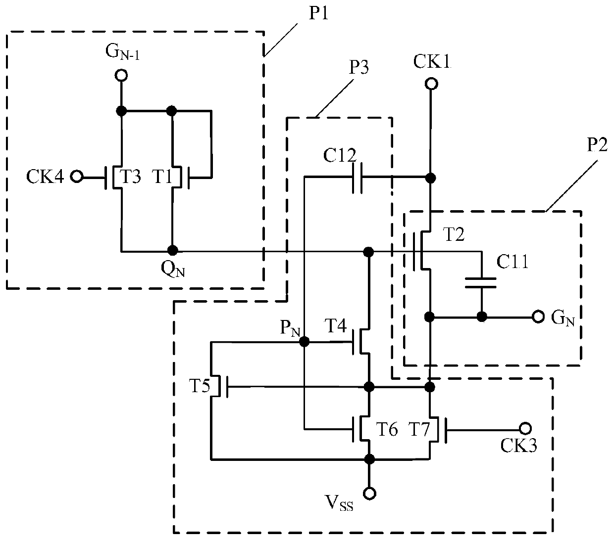
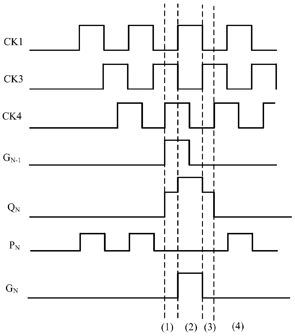
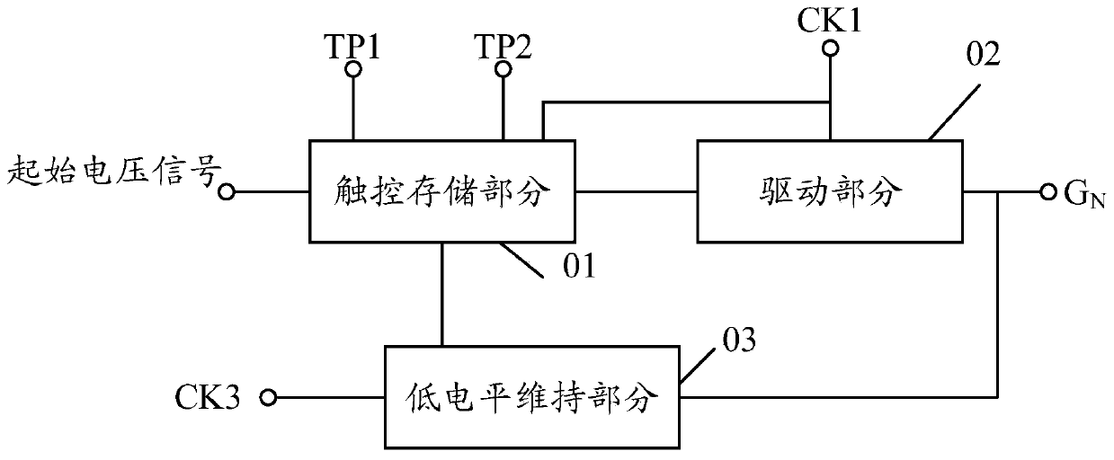
[0052] Please refer to image 3 , image 3 It is a schematic structural diagram of a gate driving circuit unit provided by an embodiment of the present application, which includes a touch storage part 01 , a driving part 02 and a low level maintaining part 03 , which will be described in detail below. The touch storage part 01 is used to respond to a first synchronous signal TP1, receive and store an initial voltage signal in the scanning sampling phase, maintain the initial voltage signal in the touch sensing phase, and respond to a second synchronous signal TP2, The starting voltage signal is sent out during the charge transfer phase. The driving part 02 is used to receive the initial voltage signal during the charge transfer phase, so as to raise the gate potential of the driving part 02 to a high level, and respond to the first clock signal CK1 to pull up Phase output scan signal G N , where the scan signal G N It can be fed back to the gate potential of the driving pa...
Embodiment 2
[0091] The present application provides a gate drive circuit, including N-level cascaded gate drive circuit units as described above, a first clock line, a second clock line, a third clock line, a first synchronization signal line, a second synchronization A signal line and a start signal line; where N is a positive number greater than 0, and n is a positive integer greater than 0 and less than N; the start signal line is used to provide an initial voltage signal for the first-level gate drive circuit unit, so The first clock line, the second clock line and the third clock line are respectively used to provide the gate drive circuit unit with a first clock signal CK1, a second clock signal CK2 and a third clock signal CK3; The first synchronization signal line is used to provide the first synchronization signal TP1 for the gate drive circuit unit; the second synchronization signal line is used to provide the second synchronization signal TP2 for the gate drive circuit unit; the...
Embodiment 3
[0095] The present application provides a touch display screen, including the gate driving circuit described in any one of the embodiments herein.
PUM
 Abstract
Description
Claims
Application Information
 - R&D Engineer
- R&D Manager
- IP Professional
- Industry Leading Data Capabilities
- Powerful AI technology
- Patent DNA Extraction
Browse by: Latest US Patents, China's latest patents, Technical Efficacy Thesaurus, Application Domain, Technology Topic, Popular Technical Reports.
© 2024 PatSnap. All rights reserved.Legal|Privacy policy|Modern Slavery Act Transparency Statement|Sitemap|About US| Contact US: help@patsnap.com