System-in-package method and device

A system-level packaging and packaging method technology, applied in the semiconductor field, can solve problems such as complex process and achieve good shielding effect

Active Publication Date: 2019-08-06
通富通科(南通)微电子有限公司
View PDF9 Cites 6 Cited by
  • Summary
  • Abstract
  • Description
  • Claims
  • Application Information

AI Technical Summary

Problems solved by technology

[0004] The inventors of the present application found in the long-term research process that the above method needs to use laser etching to form grooves, and the process is relatively complicated.

Method used


Image

  • System-in-package method and device
  • System-in-package method and device
  • System-in-package method and device

Examples


Embodiment Construction

[0025] The following will clearly and completely describe the technical solutions in the embodiments of the present application with reference to the drawings in the embodiments of the present application. Obviously, the described embodiments are only some of the embodiments of the present application, not all of them. Based on the embodiments in this application, all other embodiments obtained by persons of ordinary skill in the art without making creative efforts belong to the scope of protection of this application.

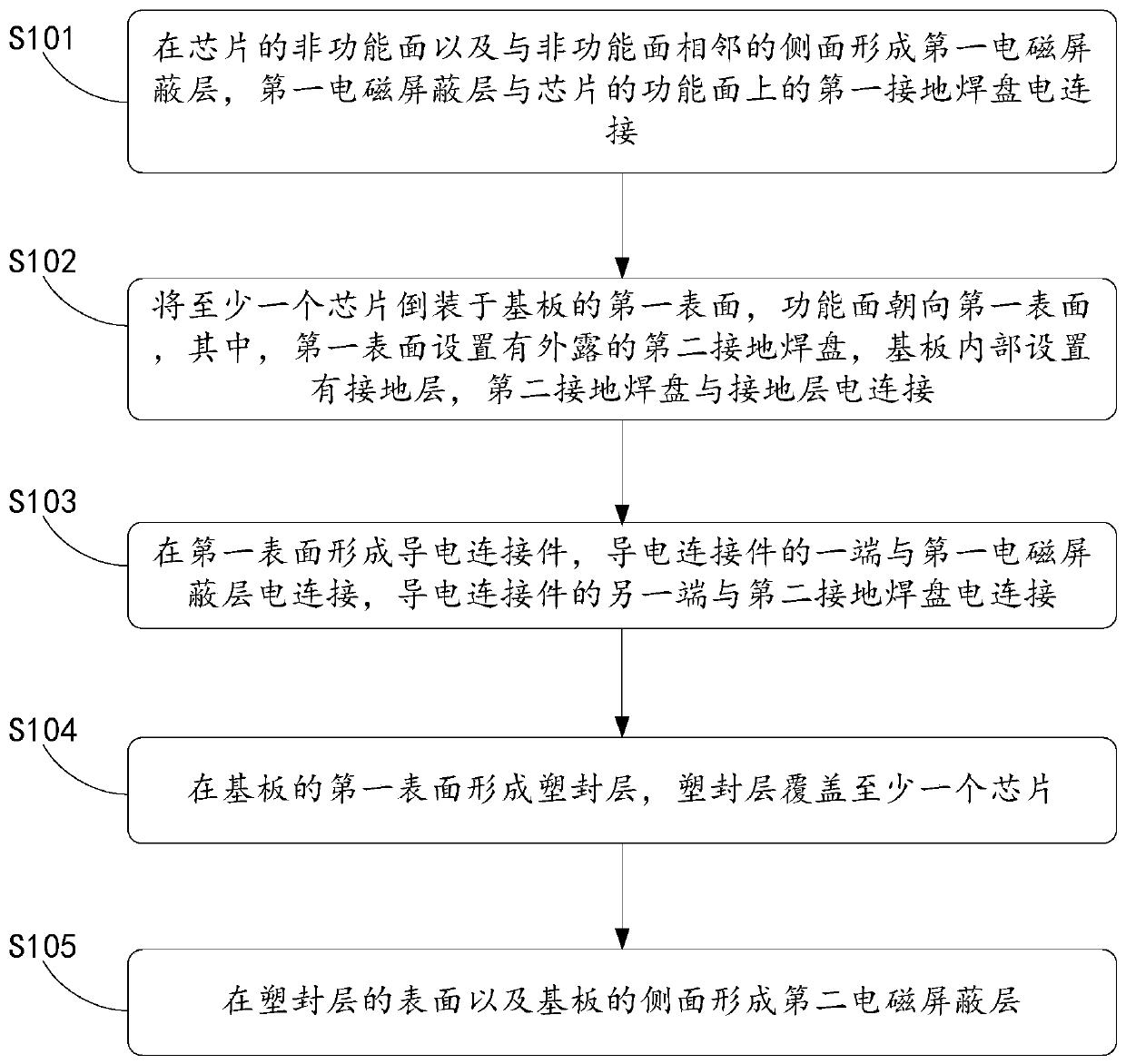
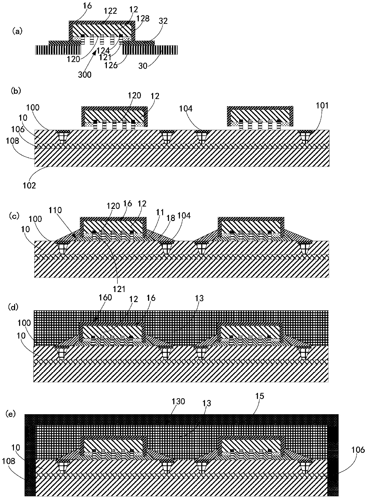
[0026] see Figure 1-Figure 2 , figure 1 It is a schematic flowchart of an embodiment of the system-in-package method of the present application, figure 2 for figure 1 A schematic structural diagram of an embodiment corresponding to step S101-step S105, the packaging method includes:

[0027] S101: Form the first electromagnetic shielding layer 16 on the non-functional surface 120 of the chip 12 and the side surface 128 adjacent to the non-functional surfa...


PUM


Abstract

The invention discloses a system-in-package method and device. The system-in-package method comprises the steps of forming a first electromagnetic shielding layer on a non-functional surface and a side surface adjacent to the non-functional surface of a chip, wherein the first electromagnetic shielding surface is electrically connected with a first grounding pad on a functional surface of the chip; mounting at least one chip on the first surface of a substrate in an inverted manner, wherein the functional surface faces towards the first surface, the first surface is provided with an exposed second grounding pad, the substrate is internally provided with a grounding layer, and the second grounding pad is electrically connected with the grounding layer; and forming a conductive connecting piece on the first surface, wherein one end of the conductive connecting piece is electrically connected with the first electromagnetic shielding layer, and the other end of the conductive connecting piece is electrically connected with the second grounding pad. The manufacturing process for realizing the electromagnetic shielding between chips can be simplified according to the method.

Description

technical field [0001] The present application relates to the field of semiconductor technology, in particular to a system-in-package method and a packaged device. Background technique [0002] System-in-package (system in package, SiP) is to package a variety of different types of chips (eg, high-speed digital circuits, analog circuits, radio frequency circuits, etc.) in a packaged device to achieve high integration requirements. As the distance between chips is getting closer, the problem of electromagnetic interference between chips is becoming more and more prominent. [0003] In order to solve the problem of electromagnetic interference between chips, Albert Lin et al. proposed a solution in the article "electrical performance characterization for novel multiple compartments shielding and verification on LTE modem SiP": first, the entire system-in-package device is plastic-encapsulated, and then the laser is used to The groove is etched, and finally the groove is fille...

Claims


Application Information

Patent Timeline
Patent Type & Authority Applications(China)
IPC IPC(8): H01L21/56H01L23/31H01L23/552
CPCH01L23/552H01L23/3121H01L21/56H01L2224/73204
Inventor 张志龙林伟江伟黄金鑫
Owner 通富通科(南通)微电子有限公司
Why Eureka
Try Eureka