
Method of making wiring board with interposer and electronic component incorporated with base board

A technology of electrical components and base boards, which is applied in the manufacture of printed circuits connected with non-printed electrical components, electrical components, printed circuits, etc., can solve problems such as limited electrical efficiency, improve electrical characteristics, and increase wiring flexibility degree of effect

Inactive Publication Date: 2019-08-02
BRIDGE SEMICON
View PDF0 Cites 0 Cited by
  • Summary
  • Abstract
  • Description
  • Claims
  • Application Information

AI Technical Summary

Problems solved by technology

However, since there are no electrical components such as capacitors, decoupling capacitors or resistors in the circuit board, the electrical performance is limited.

Method used


Image

  • Method of making wiring board with interposer and electronic component incorporated with base board
  • Method of making wiring board with interposer and electronic component incorporated with base board
  • Method of making wiring board with interposer and electronic component incorporated with base board

Examples


Embodiment 2

[0091] Figure 18-22 It is a diagram of the manufacturing method of the circuit board with the bottom circuit layer in the second embodiment of the present invention.

[0092] For the purpose of brief description, any descriptions in the above-mentioned embodiment 1 that can be used for the same application are incorporated here, and it is not necessary to repeat the same descriptions.

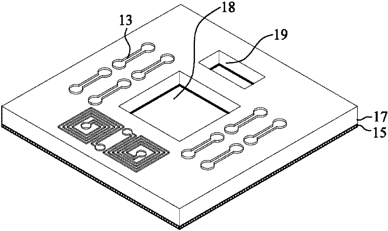
[0093] Figure 18 It is a schematic cross-sectional view of the interposer 20 and the electrical element 30 respectively disposed in the first through opening 18 and the second through opening 19 of the base board 10 . The base plate 10 is similar to figure 1 The structure shown differs in that it also includes metallized vias 14 in the core layer 17 . The metallized via 14 extends through the core layer 17 to provide an electrical connection between the top wiring layer 13 and the bottom metal film 15 .

[0094] Figure 19 It is a schematic cross-sectional view of forming the dielectric ...

Embodiment 3

[0106] Figure 30 It is a schematic cross-sectional diagram of a circuit board according to the third embodiment of the present invention, and its dielectric layer also covers the top surface of the interposer.


PUM


Abstract

A wiring board includes an interposer and an electronic component laterally surrounded by a base board and a dielectric layer and connected to a routing circuitry. The interposer and the electronic component are inserted into a first through opening and a second through opening of the base board, respectively. The dielectric layer covers the top side of the base board and the top surface of the electronic component, and fills in gaps between the interposer and the base board and between the electronic component and the base board. The routing circuitry is deposited on the dielectric layer andelectrically connected to the electronic component and a top wiring layer of the base board.

Description

technical field [0001] The invention relates to a method for making a circuit board, in particular to a method for making a circuit board provided with an intermediary layer, electrical components and a base plate. Background technique [0002] High-speed semiconductor components such as multi-chip modules usually require high-performance circuit boards to interconnect signals. However, when the power is increased, the large amount of heat generated by the semiconductor chip will degrade the performance of the device and also cause thermal stress to the chip. Accordingly, ceramic materials such as alumina or aluminum nitride are often considered suitable materials for such applications because they are thermally conductive and electrically insulating, and have a low coefficient of thermal expansion (CTE). US Pat. Nos. 8,895,998 and 7,670,872 have disclosed various circuit boards, which use ceramics as the chip pad material to achieve better reliability. However, since no e...

Claims


Application Information

Patent Timeline
Patent Type & Authority Applications(China)
IPC IPC(8): H05K1/18H05K3/28
CPCH05K1/185H05K3/284
Inventor 林文强王家忠
Owner BRIDGE SEMICON
Learn More