Circuit substrate, laminated semiconductor assembly, and manufacturing method thereof
A manufacturing method and technology for circuit substrates, which are applied in semiconductor/solid-state device manufacturing, semiconductor devices, semiconductor/solid-state device components, etc., can solve problems such as peeling, component failure, solder deformation, etc., and achieve the effect of improving wiring flexibility
- Summary
- Abstract
- Description
- Claims
- Application Information
AI Technical Summary
Problems solved by technology
Method used
Image
Examples
Embodiment 1
[0105] Figure 1-16In the first embodiment of the present invention, a diagram of a manufacturing method of a semiconductor assembly, which includes a plurality of metal leads, a metal pad, a metal film, a resin compound, a semiconductor element, a plurality of bonding wires and a molding material.
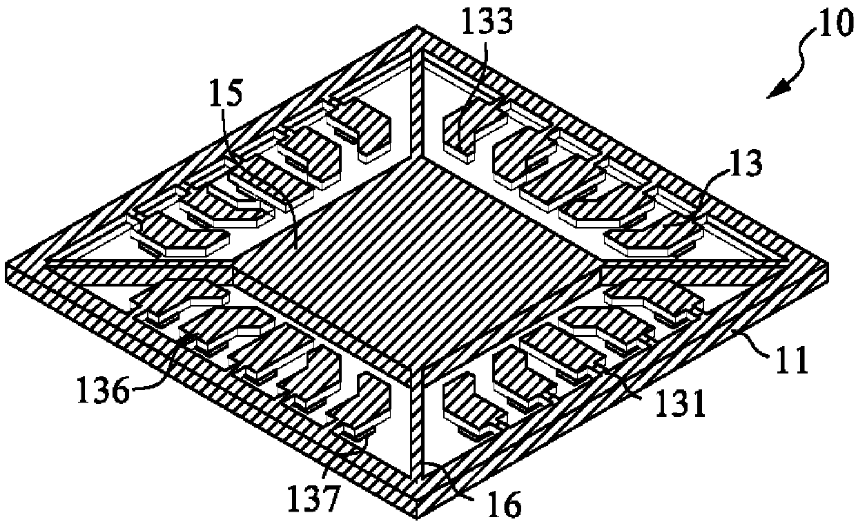
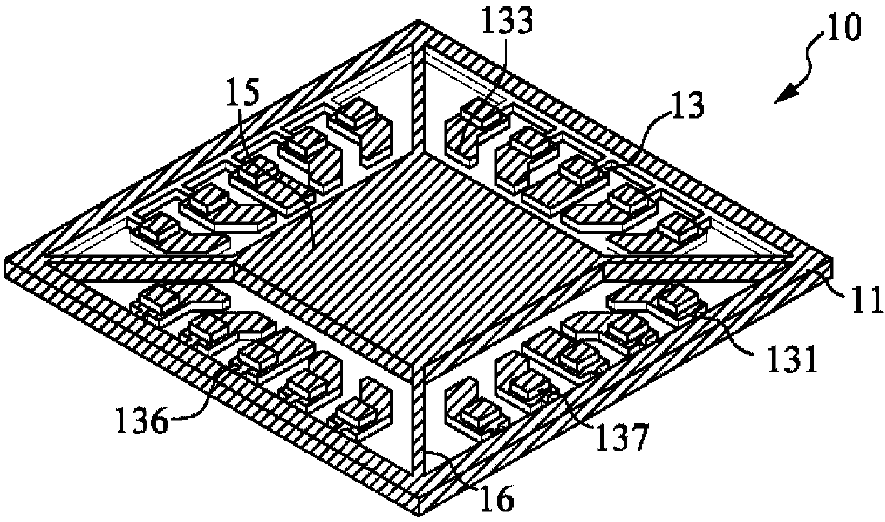
[0106] figure 1 , figure 2 and image 3 They are a schematic cross-sectional view, a top perspective view and a bottom perspective view of the patterned metal plate 10, respectively. The patterned metal plate 10 is usually made of copper alloy, steel or alloy 42, which can be formed by wet etching or stamping / punching process on rolled metal strip. , wherein the rolled metal strip has a thickness ranging from about 0.15 mm to about 1.0 mm. Here, the etching process can be performed from one side or both sides to etch through the metal strip, and the metal strip is made into a patterned metal plate 10 with a predetermined overall pattern, which includes a metal frame 11, a pl...
Embodiment 2
[0129] Figure 38-45 It is a diagram of the fabrication method of the circuit substrate with the top build-up circuit in the second embodiment of the present invention.
[0130] For the purpose of brief description, any narration that can be used for the same application in the above-mentioned embodiment 1 is all incorporated here, and need not repeat same narration again.
[0131] Figure 38 and Figure 39 respectively Figure 4 Schematic cross-sectional view and bottom perspective view of the structure after the metal frame 11 is removed. The metal frame 11 can be removed by various methods including chemical etching, mechanical trimming / cutting or sawing. By separating the metal frame 11, the connection between the metal leads 13 can be severed. Accordingly, the patterned metal plate 10 includes metal leads 13 , metal blocks 15 and connecting rods 16 .
[0132] Figure 40 and Figure 41 A schematic cross-sectional view and a perspective view of the bottom of the die...
Embodiment 3
[0140] Figure 50-61 It is a diagram of the manufacturing method of the semiconductor assembly in which the semiconductor element is attached to the resin pad in the third embodiment of the present invention.
PUM
 Abstract
Description
Claims
Application Information
 - Generate Ideas
- Intellectual Property
- Life Sciences
- Materials
- Tech Scout
- Unparalleled Data Quality
- Higher Quality Content
- 60% Fewer Hallucinations
Browse by: Latest US Patents, China's latest patents, Technical Efficacy Thesaurus, Application Domain, Technology Topic, Popular Technical Reports.
© 2025 PatSnap. All rights reserved.Legal|Privacy policy|Modern Slavery Act Transparency Statement|Sitemap|About US| Contact US: help@patsnap.com


