
Photoelectric sensor based on copper-doped cadmium sulfide nanowires and preparation method of photoelectric sensor

A photoelectric sensor, nanowire technology, applied in cadmium sulfide, nanotechnology for materials and surface science, nanotechnology, etc., can solve the problems of raw material waste, poor temperature controllability, low deposition efficiency, etc., and achieve no surface pollution. , The effect of less crystal defects and small device size

Active Publication Date: 2019-07-23
范佳旭
View PDF8 Cites 0 Cited by
  • Summary
  • Abstract
  • Description
  • Claims
  • Application Information

AI Technical Summary

Problems solved by technology

However, in the deposition process of this equipment, the design of the tube furnace only relies on the natural temperature difference formed between the middle position and the inlet and outlet positions to achieve evaporation and deposition, the temperature controllability is poor, and the steam is distributed in the entire space of the tube furnace , only a small part of which can be deposited on the substrate to form nanowires, and there are problems such as low deposition efficiency and easy waste of raw materials.

Method used


Image

  • Photoelectric sensor based on copper-doped cadmium sulfide nanowires and preparation method of photoelectric sensor
  • Photoelectric sensor based on copper-doped cadmium sulfide nanowires and preparation method of photoelectric sensor
  • Photoelectric sensor based on copper-doped cadmium sulfide nanowires and preparation method of photoelectric sensor

Examples


Embodiment 1

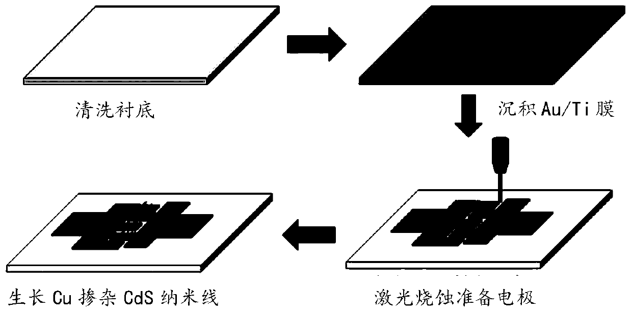
[0021] The method process used in the present invention is as figure 1 As shown, including cleaning the substrate, depositing Au / Ti film, preparing electrodes by laser ablation and growing Cu-doped CdS nanowires, the specific steps are as follows:

[0022] (1) With the alumina ceramic sheet as the substrate, it was cleaned with ethanol, acetone, and deionized water successively, and then dried with nitrogen gas. The hollow mask was used to cover, and several "cross" shapes were deposited on the surface of the substrate by electron beam evaporation. Au / Ti film array, the thickness of the metal layer is Au: 20nm, Ti: 100nm.

[0023] (2) Take out the substrate, use a UV laser marking machine to ablate and carve an insulating groove in the middle of the Au / Ti film along the set square wave route, with a width of about 4 μm, and prepare two rows of interdigitated electrodes on the metal film . A single electrode has a width of about 10 μm and a length of 30 μm.

[0024] (3) Cu-d...


PUM

PropertyMeasurementUnit
thicknessaaaaaaaaaa
widthaaaaaaaaaa
lengthaaaaaaaaaa

Abstract

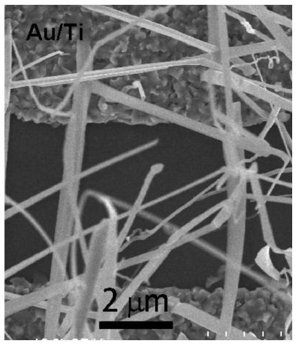
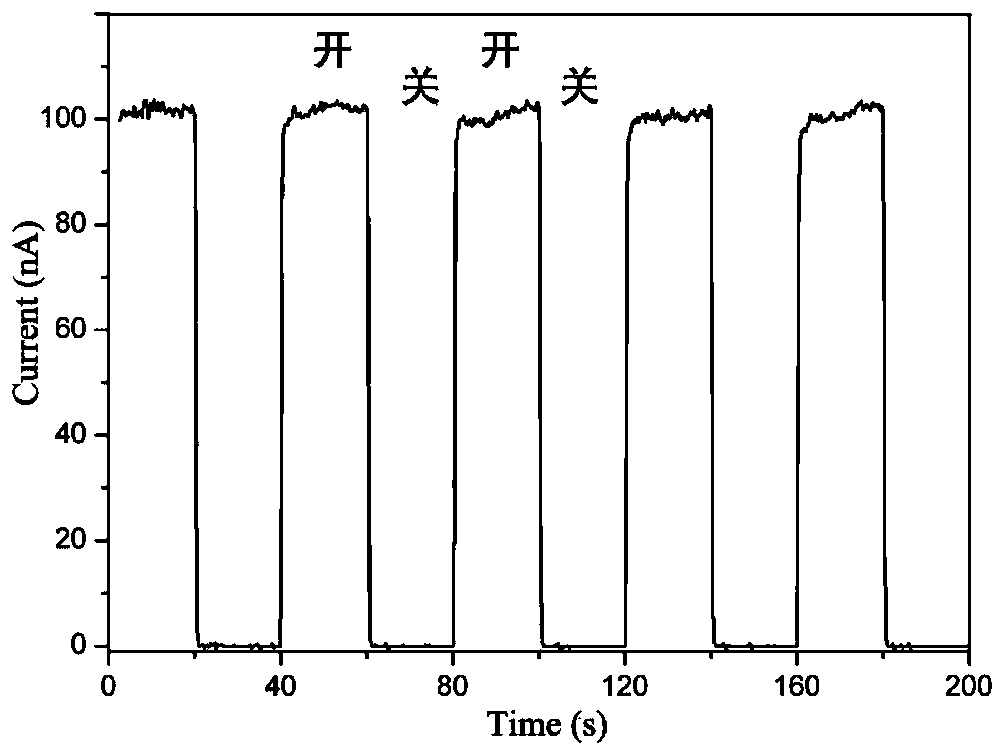
The invention discloses a photoelectric sensor based on copper-doped cadmium sulfide nanowires and a preparation method of the photoelectric sensor. The preparation method comprises the following steps: cleaning a substrate material, blow-drying with nitrogen, placing a mask, and depositing a Ti film and an Au film in sequence in a vacuum cavity by using an electron beam evaporation method; usinga UV laser marking machine to ablate and carve a groove in the Au / Ti film along a set square-wave-shaped route, and constructing an interdigital electrode; putting a substrate into gas-phase growth equipment, preparing Cu-doped CdS nanowires by using Au as a catalyst through a high-temperature gas-phase growth method, wherein according to the filling amount of a doped raw material, the percentageof Cu atoms doped into CdS is enabled to be 0-7 percent; and overlapping and bridging the nanowires one another at the top of the groove to form a photoelectric sensor unit; according to the present invention, the photoelectric sensor has characteristics of few crystal defects, no surface pollution and current transmission according to the one-dimensional path, and the gas-phase growth equipment is used to achieve the efficient growth of the nanowire steam.

Description

technical field [0001] The invention belongs to the technical field of new materials used in optoelectronics and its preparation, and in particular relates to a photoelectric sensor based on copper-doped cadmium sulfide nanowires and a preparation method thereof. Background technique [0002] Cadmium sulfide (CdS) has a band gap of 2.4eV, can absorb ultraviolet and visible light with a wavelength less than 520nm, and has a strong photoconductive effect, so it is an excellent window material. Among II-VI compounds, it is an optoelectronic material with great research potential. With the development of thin film preparation technology, CdS thin films can be prepared cheaply and on a large scale, so that the research and application of CdS in thin films has been continuously developed. Elemental doping of semiconductor materials is an effective means to adjust the band gap, electrical conductivity, and semiconductor type of materials. Doping some elements into the CdS crystal...

Claims


Application Information

Patent Timeline
Patent Type & Authority Applications(China)
IPC IPC(8): H01L31/18H01L21/02H01L31/0296H01L31/09B82Y30/00B82Y40/00C01G11/02
CPCB82Y30/00B82Y40/00C01G11/02C01P2004/16H01L21/02425H01L21/02557H01L21/0257H01L31/02963H01L31/09H01L31/1836Y02P70/50
Inventor 范佳旭
Owner 范佳旭
Learn More