Integrated micro cavity-based spectral detection chip and reconstruction method
A spectral detection and integrated microcavity technology, applied in the field of integrated microcavity spectral detection chips, can solve the problems of detector chip damage, complex process, and difficulty in restoring the spectral solution of the sample, avoiding irreversible damage and ensuring resolution. Effect
- Summary
- Abstract
- Description
- Claims
- Application Information
AI Technical Summary
Problems solved by technology
Method used
Image
Examples
Embodiment 1
[0041] In this embodiment, we demonstrate a spectral detection chip in the visible light band and a method for fabricating a stepped intermediate cavity layer by using ultraviolet nanoimprinting technology.
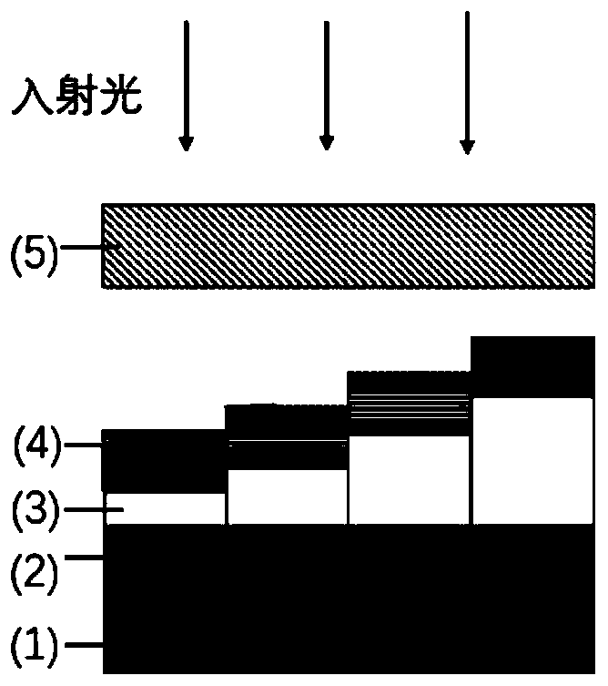
[0042] Chip-scale spectrometer structure such as figure 1 As shown, among them: 1 is an ordinary array detector, where black and white CCD chips are selected; 2 is the first dielectric high-reflection film, and the material selected is Ta 2 o 5 and SiO 2 ; 3 is a two-dimensional stepped intermediate cavity layer made by ultraviolet nanoimprinting technology; 4 is a second dielectric high-reflection film, and the selected material is Ta 2 o 5 and SiO 2 ; 5 is a bandpass filter.
[0043] Dielectric reflection film 2 structure is: λ=633nm, H-Ta 2 o 5 ,L-SiO 2 , (LH) 5 1.4L.
[0044] Dielectric reflection film 4 structure is: λ=633nm, H-Ta 2 o 5 ,L-SiO 2 , (HL) 5 .
[0045] The stepped intermediate cavity layer 3 is a two-dimensional grid stepped dielectric la...
Embodiment 2
[0058] In this embodiment, we demonstrate a spectral detection chip in the visible light band and a method for fabricating a stepped intermediate cavity layer by thermal nanoimprinting technology.
[0059] Chip-scale spectrometer structure such as figure 1 As shown, among them: 1 is an ordinary array detector, where black and white CCD chips are selected; 2 is the first dielectric high-reflection film, and the material selected is Ta 2 o 5 and SiO 2 ; 3 is a two-dimensional stepped intermediate cavity layer made by ultraviolet nanoimprinting technology; 4 is a second dielectric high-reflection film, and the selected material is Ta 2 o 5 and SiO 2 ; 5 is a bandpass filter.
[0060] Dielectric reflection film 2 structure is: λ=633nm, H-Ta 2 o 5 ,L-SiO 2 , (LH) 5 1.4L.
[0061] Dielectric reflection film 4 structure is: λ=633nm, H-Ta 2 o 5 ,L-SiO 2 , (HL) 5 .
[0062] The stepped intermediate cavity layer 3 is a two-dimensional grid stepped dielectric layer. In th...
Embodiment 3
[0075] In this embodiment, we demonstrate a spectral detection chip in the infrared band and a method for fabricating a stepped intermediate cavity layer by using ultraviolet nanoimprinting technology.
[0076] Chip-scale spectrometer structure such as figure 1 As shown, among them: 1 is the infrared area detector, and the low-temperature mercury cadmium telluride infrared detector chip is used here; 2 is the first dielectric high-reflection film, and the materials are Si and SiO; 3 is the ultraviolet nanoimprint technology middle cavity layer; 4 is the second dielectric high-reflection film, and the selected materials are Si and SiO; 5 is a bandpass filter.
[0077] Detector 1 uses the MARS MW detector chip and corresponding components from Sofradia, France.
[0078] Dielectric reflection film 2 structure is: λ=3833nm, H-Si, L-SiO, (LH) 5 1.4L.
[0079] Dielectric reflection film 4 structure is: λ=3833nm, H-Si, L-SiO, (HL) 5 .
[0080] The stepped intermediate cavity la...
PUM
 Abstract
Description
Claims
Application Information
 - R&D
- Intellectual Property
- Life Sciences
- Materials
- Tech Scout
- Unparalleled Data Quality
- Higher Quality Content
- 60% Fewer Hallucinations
Browse by: Latest US Patents, China's latest patents, Technical Efficacy Thesaurus, Application Domain, Technology Topic, Popular Technical Reports.
© 2025 PatSnap. All rights reserved.Legal|Privacy policy|Modern Slavery Act Transparency Statement|Sitemap|About US| Contact US: help@patsnap.com


