Semiconductor device and method for manufacturing same

A manufacturing method, semiconductor technology, applied in the direction of semiconductor/solid-state device manufacturing, semiconductor devices, semiconductor/solid-state device components, etc., can solve problems such as poor moisture resistance, difficulty in ensuring solderability, poor connection reliability, etc., to ensure Solderability, quality and reliability improvement effects

Active Publication Date: 2019-07-12
AOI ELECTRONICS CO LTD
View PDF8 Cites 1 Cited by
  • Summary
  • Abstract
  • Description
  • Claims
  • Application Information

AI Technical Summary

Problems solved by technology

[0009]Leadless package is singulated by cutting the lead terminals and mold compound (MoldCompound) with a dicing saw, so although the lead terminals The lower surface of the lead terminal is covered with a solder-wetting material, but the side of the lead terminal is not covered with a solder-wetting material. When thermally mounting the mounting substrate with a solder material, the connection reliability of the outer lower end of the side lead is poor. In addition, , visual inspection of solder joints is also difficult
[0010] That is, after overmolding the outer lower portion of the side pins with molding compound (to form a step at the tie bar of the lead frame), the Removal of the molding compound does not completely remove the molding compound, and the subsequent coverage of the solder-wetting material becomes uneven, making it difficult to ensure solderability
[0011] In addition, when using a laser to remove the mold compound, due to the laser on the outer lower end of the side pin Excessive exposure, thus creating cavitated parts of the molded resin on both sides of the terminal, which may deteriorate moisture resistance

Method used


Image

  • Semiconductor device and method for manufacturing same
  • Semiconductor device and method for manufacturing same
  • Semiconductor device and method for manufacturing same

Examples


Embodiment Construction

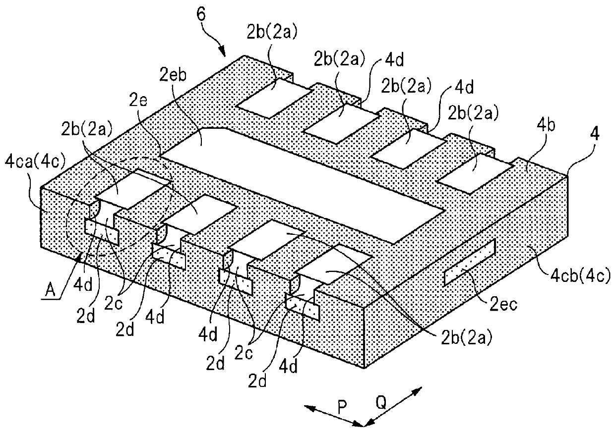
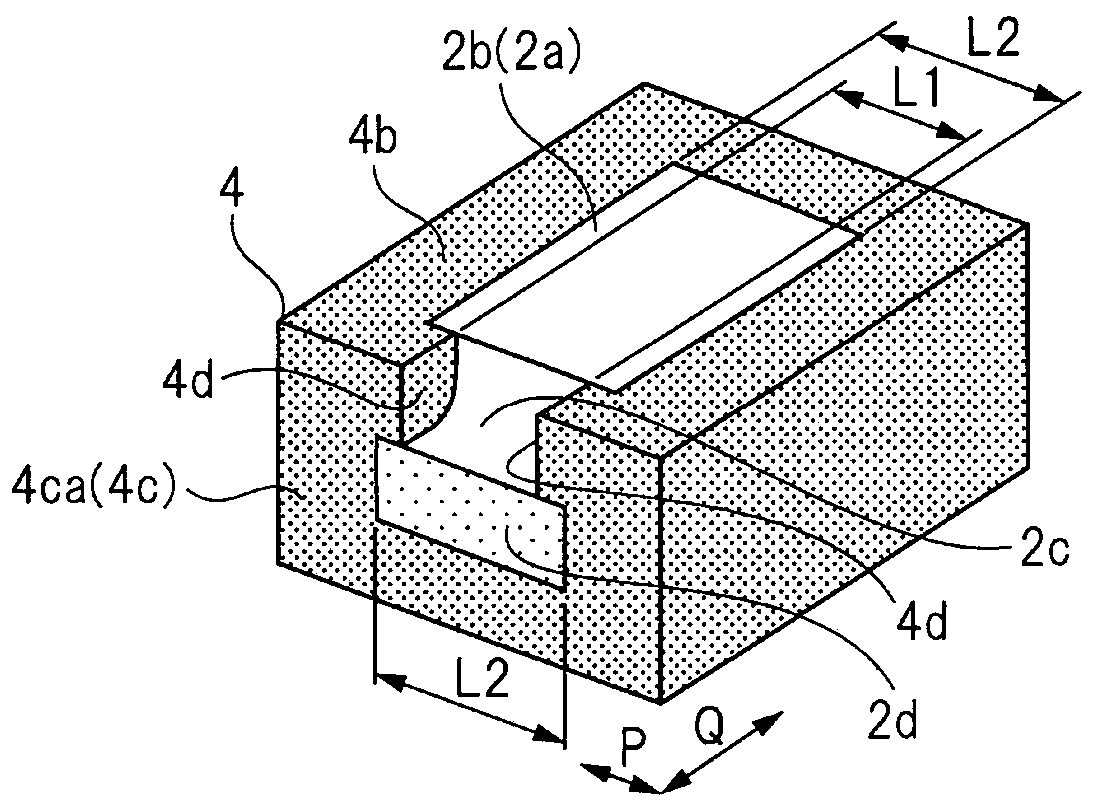
[0080] figure 1 It is a perspective view showing an example of the structure on the mounting surface side of the semiconductor device according to the embodiment of the present invention, figure 2 is showing figure 1 An enlarged partial perspective view of the structure of Part A.

[0081]

[0082] figure 1 The shown semiconductor device according to this embodiment is a leadless package assembled by the so-called MAP method in which the package is diced and singulated during assembly. In this embodiment, a description will be given using DFN (Dual-Flat No-leads: Dual-Flat No-leads) 6 as an example of a leadless package assembled by the above-mentioned MAP method. DFN6 is a semiconductor package in which a plurality of lead portions 2a are arranged along each of two opposing side surfaces 4ca of a sealing body 4 made of resin, and a terminal portion 2b of each lead portion 2a is arranged on the sealing body 4 as on the back 4b of the mounting surface.

[0083] The deta...


PUM


Abstract

The invention provides a semiconductor device and a method for manufacturing the same, wherein the solderability of a pin part of the semiconductor device without a pin is ensured. A DFN (6) is provided with a semiconductor chip; a die pad; a plurality of pin parts (2a) arranged around the die pad and having notches (2c) formed at the tips of the pin parts; and a plurality of leads which electrically connect the surface electrode of the semiconductor chip and one of the plurality of pin parts (2a), and a resin sealing body (4) which covers the semiconductor chip and a part of each of the plurality of pin parts (2a). Furthermore, each of the plurality of pin parts (2a) has a terminal part (2b) exposed on the back surface (4b) of the sealing body (4), and the width of the cutout part (2c) inthe direction along the arrangement direction (P) of the plurality of pin parts (2a) is smaller than the width of the terminal part (2b) in the direction along the arrangement direction (P).

Description

technical field [0001] The present invention relates to, for example, a leadless type semiconductor device and its manufacturing technology. Background technique [0002] A method of manufacturing a semiconductor device called MAP (Mold Array Package) is known. In this method, a sealing body is used to uniformly cover a plurality of device regions, and dicing is performed for each sealing body (package dicing: Package Dicing). Monolithic. [0003] As a method of manufacturing MAP, for example, US Patent No. 8017447 specification (Patent Document 1) discloses a technique of overmolding a lead frame (Lead Frame) connected to an adjacent structure and formed with a connecting rod. , to remove the molding material filling the groove by irradiating laser light on the groove in which the connecting rod is formed. [0004] In addition, for example, JP-A-2013-143445 (Patent Document 2) discloses a technique of irradiating laser beams to leads exposed from the lower surface of a se...

Claims


Application Information

Patent Timeline
Patent Type & Authority Applications(China)
IPC IPC(8): H01L23/495H01L23/31H01L21/50H01L21/56
CPCH01L23/49541H01L23/3114H01L21/50H01L21/56
Inventor 成田亨海老名建志小野哲弥
Owner AOI ELECTRONICS CO LTD
Why Eureka
Try Eureka