Reverse terminal structure of bidirectional withstand voltage power device based on step etching in drift region

A technology of power devices and terminal structures, which is applied in semiconductor devices, electrical components, circuits, etc., can solve problems such as difficult to apply SiC material process, increase conduction power consumption of series diodes, influence of package parasitic parameters, etc., to avoid avalanche strikes The effect of wear, reduction of electric field, and reduction of charge flux

Active Publication Date: 2021-12-10
INST OF ELECTRONICS ENG CHINA ACAD OF ENG PHYSICS
View PDF11 Cites 0 Cited by
  • Summary
  • Abstract
  • Description
  • Claims
  • Application Information

AI Technical Summary

Problems solved by technology

However, although the above reverse termination structures have been well applied in Si-based power devices, these termination structures are still difficult to realize in the fabrication of SiC high-voltage devices.
The main difficulty is that the diffusion process and deep etching process commonly used in the production of Si-based power devices are still difficult to apply to the processing of SiC materials.
The current common method for SiC power devices to achieve bidirectional withstand voltage is to use series diodes to withstand reverse blocking high voltage. Negative impact

Method used


Image

  • Reverse terminal structure of bidirectional withstand voltage power device based on step etching in drift region
  • Reverse terminal structure of bidirectional withstand voltage power device based on step etching in drift region
  • Reverse terminal structure of bidirectional withstand voltage power device based on step etching in drift region

Examples


Embodiment 1

[0022] The reverse terminal structure of the bidirectional withstand voltage power device based on step etching in the drift region designed in this embodiment, such as figure 1 As shown, it includes a P-type semiconductor drift region 1 and an N-type semiconductor region 2 below it. The N-type semiconductor region 2 is a substrate layer and has a stepped structure at the edge of the drift region 1 with four steps.

[0023] In this embodiment, the ratio of the depth to the width of each step is a fixed value. The sum of the depths of each step is greater than the thickness of the P-type semiconductor drift region 1 , that is, the lowest step is formed jointly by the N-type semiconductor region 2 and the P-type semiconductor drift region 1 . In this example, the semiconductor materials of the P-type semiconductor drift region 1 and the N-type substrate 2 are SiC materials, and may also be silicon or other semiconductor materials.

[0024] The working principle of this embodime...

Embodiment 2

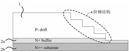
[0027] Such as figure 2 As shown, compared with Embodiment 1, the N-type semiconductor region 2 of this embodiment includes upper and lower layers, wherein the lower layer is the substrate layer 2b, the upper layer is adjacent to the semiconductor drift region 1 of the first conductivity type, and the upper layer is the buffer layer 2a , the doping concentration of the substrate layer 2b is higher than that of the buffer layer 2a. Wherein, the lowest step in the stepped structure is jointly formed by the buffer layer 2 a of the N-type semiconductor region 2 and the P-type semiconductor drift region 1 .

Embodiment 3

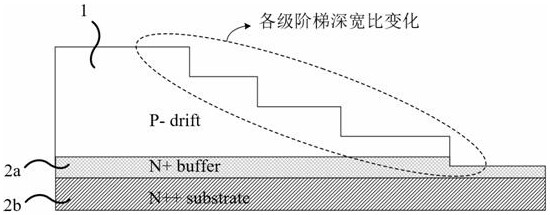
[0029] Such as image 3 As shown, compared with the embodiment 2, the step structure at the edge of the semiconductor drift region 1 of the present embodiment has a changed step aspect ratio. The width of the step near the bottom is larger than that of the top step, which is more conducive to transferring the high electric field region to the body, thereby further reducing the terminal electric field of the edge step.


PUM


Abstract

The invention belongs to the field of power semiconductor devices, and proposes a reverse terminal structure of a bidirectional withstand voltage power device based on stepwise etching of a drift region, including a semiconductor drift region of a first conductivity type and a semiconductor region of a second conductivity type below it, There is a ladder structure at the edge of the drift area, and the number of steps is ≥ 2; the ratio of the depth and width of each step can be a fixed value or a variable value. The sum of the step depths of each level is greater than the thickness of the drift region of the first conductivity type. The multi-level steps in the structure of the present invention form an equivalent positive grinding angle structure, which can effectively reduce the charge flux of the bottom PN junction in the reverse blocking state, so that the electric field in the multi-level step area of ​​the reverse terminal is significantly reduced, and this area is avoided. Avalanche breakdown occurs in the blocking state, which is also beneficial to suppress the leakage on the surface of the step, thereby improving the reverse blocking withstand voltage of the device.

Description

technical field [0001] The invention relates to a reverse terminal structure of a bidirectional withstand voltage power device based on step etching in a drift region, and belongs to the field of power semiconductor devices. Background technique [0002] Conventional power devices currently used in mainstream power electronics applications such as DC-DC and DC-AC often only have forward blocking capabilities. In AC-AC power conversion applications, the use of high-voltage power devices with bidirectional withstand voltage capabilities can save The series diode in the bidirectional switch can effectively reduce conduction loss and switching loss, and improve AC-AC power conversion efficiency. In the pulse power system, a high-voltage switching device with bidirectional withstand voltage capability is used, which can withstand the bidirectional high voltage of the positive and negative half cycles of the energy storage capacitor, so that the series diode and the anti-parallel ...

Claims


Application Information

Patent Timeline
Patent Type & Authority Patents(China)
IPC IPC(8): H01L29/06
Inventor 周坤李良辉张林李志强徐星亮李俊焘
Owner INST OF ELECTRONICS ENG CHINA ACAD OF ENG PHYSICS
Why Eureka
Try Eureka