
A gold finger laser cutting method and system for circuit boards

A laser cutting and gold finger technology, applied in laser welding equipment, metal processing equipment, welding equipment, etc., can solve problems such as carbonization of gold finger insulating materials, difficulty in meeting die-cutting requirements, and gold finger dislocation

Active Publication Date: 2021-04-27
WUHAN EXCEL SCI & TECH LTD EST
View PDF9 Cites 0 Cited by
  • Summary
  • Abstract
  • Description
  • Claims
  • Application Information

AI Technical Summary

Problems solved by technology

However, traditional CNC machining and die stamping are difficult to meet the die-cutting requirements. The lines of the gold fingers are densely distributed, and a slight deviation in the position will cause the gold fingers to be misaligned in the connection, which will lead to abnormal signal communication of the gold fingers, and thus make good products rate is not high
[0005] At present, the industry mainly adopts the method of laser cutting gold fingers, but for this kind of high-density gold fingers, whether it is ultraviolet nanosecond laser or ultra-short pulse laser, due to the different interaction mechanisms between polyimide and copper foil and laser, resulting in copper The threshold value of foil laser processing is much higher than that of polyimide, and there is a problem of carbonization of the insulating material of the gold finger, which causes a micro-short circuit between the fingers of the gold finger, affecting the quality of the gold finger and even electronic equipment

Method used


Image

  • A gold finger laser cutting method and system for circuit boards
  • A gold finger laser cutting method and system for circuit boards
  • A gold finger laser cutting method and system for circuit boards

Examples


Embodiment Construction

[0029] The principles and features of the present invention are described below in conjunction with the accompanying drawings, and the examples given are only used to explain the present invention, and are not intended to limit the scope of the present invention.

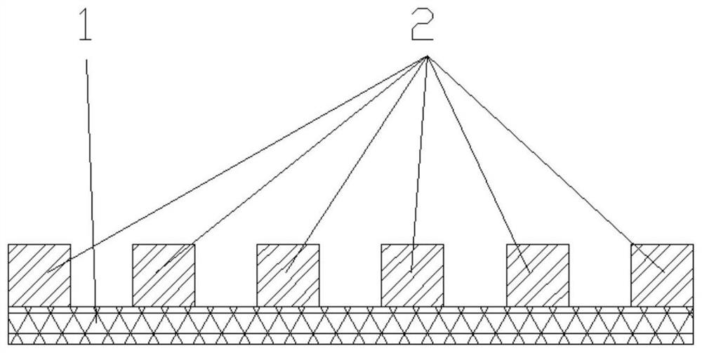
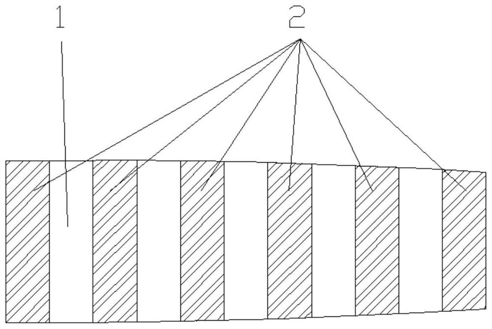
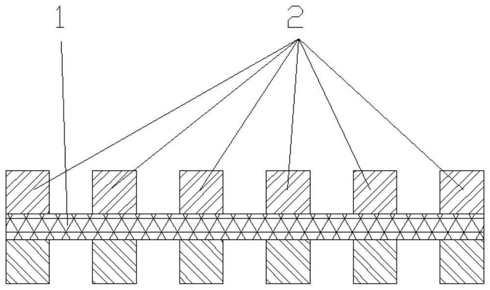
[0030] Such as figure 1 and figure 2 As shown, it is a schematic diagram of a single-sided gold finger circuit board, wherein the gold fingers 2 are usually distributed on one side of the insulating layer 1 at equal intervals. Gold finger 2 is generally a copper block with a width of 25 microns, and the surface is plated with gold to form a conductive block. The insulating layer 1 is usually made of materials such as polyimide (PI), modified polyimide (MPI), liquid crystal engineering plastic (LCP) and Teflon.

[0031] Double-sided gold finger circuit board such as image 3 As shown, the gold fingers 2 are generally formed by etching and plating double-sided copper foil, and the upper and lower surfaces of the i...


PUM

PropertyMeasurementUnit
diameteraaaaaaaaaa

Abstract

The invention relates to a gold finger laser cutting method and system for circuit boards. The method comprises: projecting the inter-finger insulating layer clearing laser beam and the golden finger cutting laser beam to the area to be cut of the circuit board for scanning processing, and the laser peak value of the projected light spot of the inter-finger insulating layer clearing laser beam on the inter-finger insulating layer to-be-cut area The power density is less than the laser processing threshold of the gold finger material, and greater than or equal to the laser processing threshold of the inter-finger insulating layer material, and the laser peak power density of the projected spot of the gold finger cutting laser beam on the gold finger to be cut area is greater than or equal to the laser processing of the gold finger material Threshold: The inter-finger insulation layer removal laser beam is used to process and form a hole in the inter-finger insulation layer to be cut area, and the golden finger cutting laser beam is used to process and form a slit on the circuit board. Outer side edge. The technical scheme of the invention can solve the micro-short circuit problem generated on the golden finger when the circuit board is cut by laser.

Description

technical field [0001] The invention relates to the technical field of laser processing, in particular to a gold finger laser cutting method and system for circuit boards. Background technique [0002] The increasing demand for portable electronic products has driven the development of circuit boards from single-sided to double-sided, multi-layer, flexible and rigid-flexible boards, and continues to develop in the direction of high precision, high density and high reliability. The base material of the flexible circuit board (FPC board) is copper, and it needs to be covered with a layer of cover film on the circuit board substrate. The material of the cover film is generally polyimide. Combined with the surface of the circuit board substrate to play a protective role. In the later stage of FPC board production, the shape needs to be processed, and there is a row of golden fingers on the shape to connect with other electronic products. [0003] The so-called gold fingers, al...

Claims


Application Information

Patent Timeline
Patent Type & Authority Patents(China)
IPC IPC(8): B23K26/38B23K26/70
Inventor 张立国
Owner WUHAN EXCEL SCI & TECH LTD EST
Learn More