Manufacture method for thin-film resistor

A technology of thin film resistors and manufacturing methods, applied in circuits, electrical components, electric solid devices, etc., can solve problems such as over-etching of thin-film resistor materials, and achieve the effects of avoiding over-etching, improving accuracy and reliability

Inactive Publication Date: 2019-06-18
SHANGHAI INTEGRATED CIRCUIT RES & DEV CENT
View PDF4 Cites 2 Cited by
  • Summary
  • Abstract
  • Description
  • Claims
  • Application Information

AI Technical Summary

Problems solved by technology

[0008] The purpose of the present invention is to overcome the above-mentioned defects in the prior art, and provide a method for manufacturing thin-film resistors to solve the problem of over-etching of thin-film resistor materials in the prior art

Method used


Image

  • Manufacture method for thin-film resistor
  • Manufacture method for thin-film resistor
  • Manufacture method for thin-film resistor

Examples


Embodiment Construction

[0030] The specific embodiment of the present invention will be further described in detail below in conjunction with the accompanying drawings.

[0031] It should be noted that, in the following specific embodiments, when describing the embodiments of the present invention in detail, in order to clearly show the structure of the present invention for the convenience of description, the structures in the drawings are not drawn according to the general scale, and are drawn Partial magnification, deformation and simplification are included, therefore, it should be avoided to be interpreted as a limitation of the present invention.

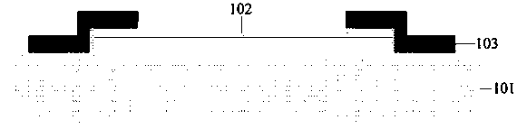
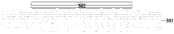
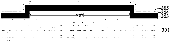
[0032] In the following specific embodiments of the present invention, please refer to figure 2 , figure 2 It is a schematic flow chart of a manufacturing method of a thin film resistor of the present invention; at the same time, please refer to Figure 3-Figure 7 , Figure 3-Figure 7 It is a schematic cross-sectional view of a device formed dur...


PUM

PropertyMeasurementUnit
thicknessaaaaaaaaaa
thicknessaaaaaaaaaa

Abstract

The invention discloses a manufacture method for a thin-film resistor. The manufacture method comprises the following steps that: S01: providing a substrate of which the surface is coated with an insulating layer; S02: depositing a thin film resistor material on the substrate, and carrying out graphics on the film resistor material; S03: depositing a metal electrode material, an etching stop layerand a hard mask in sequence on the substrate and the thin film resistor material; S04: adopting first-type dry method etching to carry out graphics on the hard mask, and removing photoresist; S05: adopting second-type dry method etching to continuously carry out graphics on the etching stop layer; and S06: adopting wet method etching to continuously carry out graphics on the metal electrode material to form the thin-film resistor. By use of the manufacture method, the problem of the over etching of the thin-film resistor and the etching residue of the metal electrode can be avoided, and the accuracy and the reliability of the thin-film resistor can be improved.

Description

technical field [0001] The present invention relates to the technical field of semiconductor processing and manufacturing, and more specifically, to a method for manufacturing thin film resistors. Background technique [0002] As the performance requirements of modern electronic equipment are getting higher and higher, the performance requirements of on-chip components are also becoming more and more stringent. In modern large-scale integrated circuit chips and sensor chips, thin-film resistors are an indispensable device, including voltage divider resistors, thermistors, photoresistors, etc. on the chip. The accuracy of thin-film resistors also directly affects the accuracy of advanced chips. and performance. [0003] figure 1 It is a schematic diagram of the main structure of a thin film resistor in the prior art. Such as figure 1 As shown, its manufacturing method mainly includes: [0004] First, a silicon wafer covered with an insulating layer is provided as a subst...

Claims


Application Information

Patent Timeline
Patent Type & Authority Applications(China)
IPC IPC(8): H01L23/64
Inventor 左青云
Owner SHANGHAI INTEGRATED CIRCUIT RES & DEV CENT
Why Eureka
Try Eureka