Trench IGBT chip
A technology of grooves and chips, applied in the direction of electrical components, circuits, semiconductor devices, etc., can solve the problems of unfavorable and impacted chip turn-on and turn-off, optimize the chip conduction voltage drop, avoid mutual interference, and reduce input and output The effect of capacitance
- Summary
- Abstract
- Description
- Claims
- Application Information
AI Technical Summary
Problems solved by technology
Method used
Image
Examples
Embodiment 1
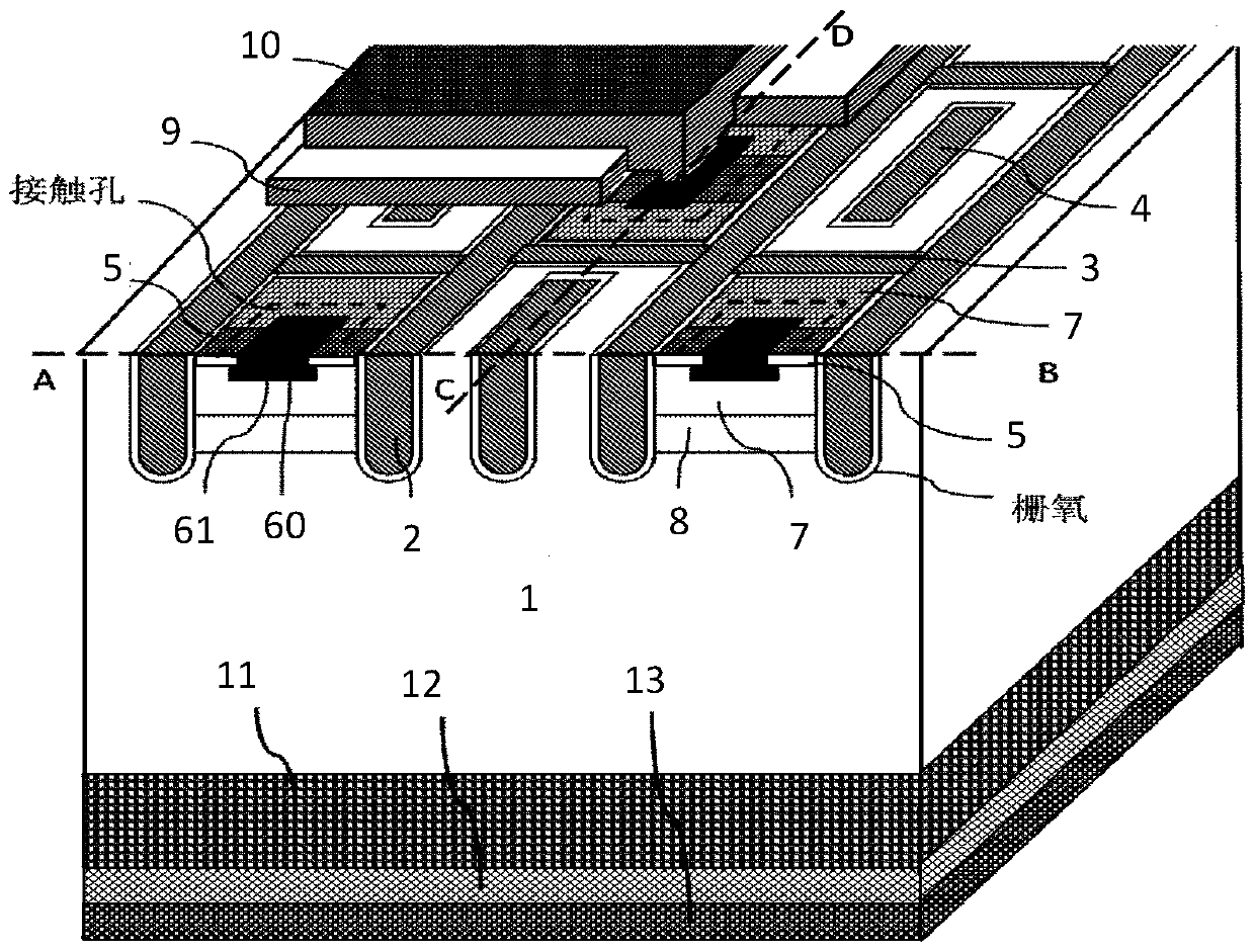
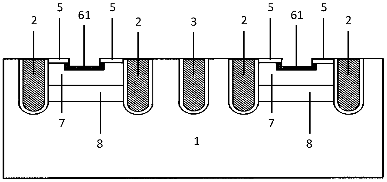
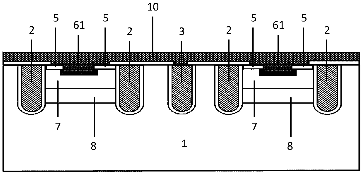
[0040] figure 1 It is a schematic structural diagram of a trench IGBT chip according to Embodiment 1 of the present invention. Such as figure 1 As shown, it may include an N-type substrate 1, a plurality of strip-shaped trench gates 2, a plurality of auxiliary gates 3, a strip-shaped accompanying gate 4, an N+ region 5, a P+ region 61, a P well region 7, and an N well Region 8, oxide layer 9, emitter metal layer 10, N-type buffer layer 11, anode P region 12 and anode metal layer 13.
[0041] A plurality of strip-shaped trench gates 2 are respectively located in a plurality of trenches etched downward from the upper surface of the N-type substrate 1 , and extend along the surface of the N-type substrate 1 and are distributed in parallel.
[0042] A plurality of auxiliary gates 3 are respectively located in a plurality of trenches formed by etching the upper surface of the N-type substrate 1 downwards, and are perpendicular to the length direction of the strip-shaped trench ga...
Embodiment 2
[0054] Figure 6 It is a schematic structural diagram of a trench IGBT chip according to Embodiment 2 of the present invention. Such as Figure 6 As shown, it may include an N-type substrate 1, a plurality of strip-shaped trench gates 2, a plurality of auxiliary gates 3, an N+ region 5, a P+ region 61, a P well region 7, an N well region 8, an oxide layer 9, Emitter metal layer 10 , N-type buffer layer 11 , anode P region 12 and anode metal layer 13 .
[0055] A plurality of strip-shaped trench gates 2 are respectively located in a plurality of trenches etched downward from the upper surface of the N-type substrate 1 , and extend along the surface of the N-type substrate 1 and are distributed in parallel.
[0056] A plurality of auxiliary gates 3 are respectively located in a plurality of trenches formed by etching the upper surface of the N-type substrate 1 downwards, and are perpendicular to the length direction of the strip-shaped trench gate 2, so that the plurality of s...
Embodiment 3
[0066] Figure 7 It is a schematic structural diagram of a trench IGBT chip according to Embodiment 3 of the present invention. Such as Figure 7 As shown, it may include an N-type substrate 1, a plurality of strip-shaped trench gates 2, a plurality of auxiliary gates 3, a strip-shaped accompanying gate 4, an N+ region 5, a P+ region 62, a P well region 7, and an N well region. Region 8, oxide layer 9, emitter metal layer 10, N-type buffer layer 11, anode P region 12 and anode metal layer 13.
[0067] A plurality of strip-shaped trench gates 2 are respectively located in a plurality of trenches etched downward from the upper surface of the N-type substrate 1 , and extend along the surface of the N-type substrate 1 and are distributed in parallel.
[0068] A plurality of auxiliary gates 3 are respectively located in a plurality of trenches formed by etching the upper surface of the N-type substrate 1 downwards, and are perpendicular to the length direction of the strip-shaped...
PUM
 Abstract
Description
Claims
Application Information
 - R&D
- Intellectual Property
- Life Sciences
- Materials
- Tech Scout
- Unparalleled Data Quality
- Higher Quality Content
- 60% Fewer Hallucinations
Browse by: Latest US Patents, China's latest patents, Technical Efficacy Thesaurus, Application Domain, Technology Topic, Popular Technical Reports.
© 2025 PatSnap. All rights reserved.Legal|Privacy policy|Modern Slavery Act Transparency Statement|Sitemap|About US| Contact US: help@patsnap.com


