


Quick Research
Generate reliable direction feasibility study reports for your R&D in just a few steps.

Technical Q&A
Discover and master advanced knowledge NOW. Basics, ideas, possibilities, all at once.

Find Solutions
As an expert in R&D theories, this can generate solutions to your technical problems instantly.

Evaluate Feasibility
Analyze your overall solution with one click, know your potential R&D risks in advance.

Monitor Landscape
Get weekly tech updates, stay abreast of the latest tech innovations and key insights.
A multi-passband complex filter circuit
A complex filter and multi-passband technology, which is applied in the direction of multi-terminal pair network and frequency selective two-terminal pair network, can solve the problems of single energy efficiency and poor flexibility, and achieve the effect of flexible use, low cost and wide application range
- Summary
- Abstract
- Description
- Claims
- Application Information
AI Technical Summary
Problems solved by technology
Method used
Image

Examples
Embodiment 1
[0016] Embodiment 1. A multi-pass band complex filter circuit
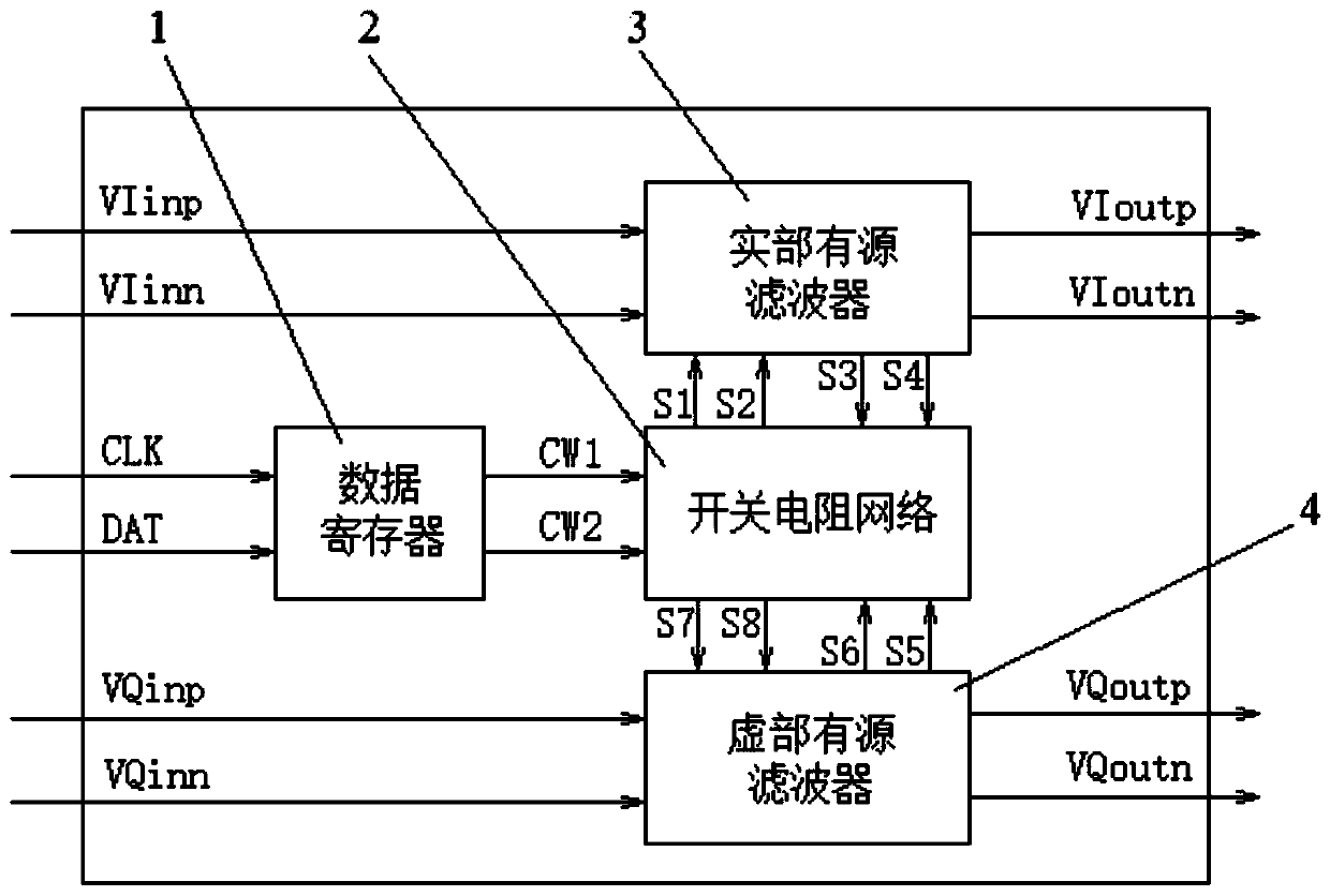
[0017] Such as figure 1 As shown, a multi-passband complex filter circuit provided by the present invention is composed of a data register 1, a switch resistor network 2, a real part active filter 3 and an imaginary part active filter 4.
[0018] The data register 1 has two input terminals and two output terminals, the two input terminals are respectively connected with the external serial bus signal CLK and DAT, and the two output terminals are connected with the two input terminals of the switch resistor network 2; The switch resistance network 2 described above has six input terminals and four output terminals, wherein two input terminals are connected with the two output terminals of the data register 1, and the other four input terminals are respectively connected with the two output terminals of the real part active filter 3. The output terminal is connected to the two output terminals of the imaginary par...
Embodiment 2
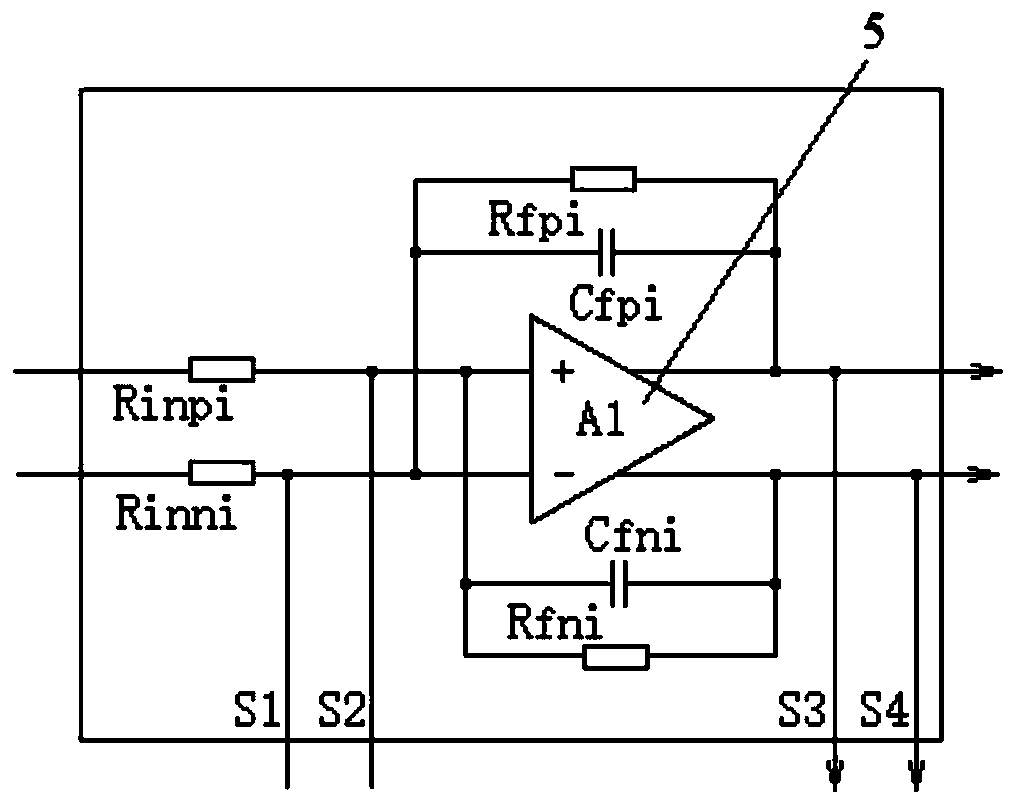
[0019] Embodiment 2, the implementation of real part active filter
[0020] Such as figure 2As shown, the real part active filter 3 is made up of the first operational amplifier 5, resistor Rinpi, resistor Rinni, resistor Rfpi, resistor Rfni, capacitor Cfpi and capacitor Cfni; wherein, the non-inverting input terminal of the first operational amplifier 5 Connect with one end of resistance Rinpi, resistance Rfni, electric capacity Cfni simultaneously, and be connected together with the output terminal (S2) of switch resistance network; One end is connected and connected with the output terminal (S1) of the switch resistor network; the other end of the resistor Rinpi and the resistor Rinni are connected with the external input signal; the resistor Rfpi and the capacitor Cfpi are connected in parallel, and connected across the same phase of the first operational amplifier 5 On the output terminal node and the inverting input terminal node; the resistor Rfni and the capacitor Cfn...
Embodiment 3
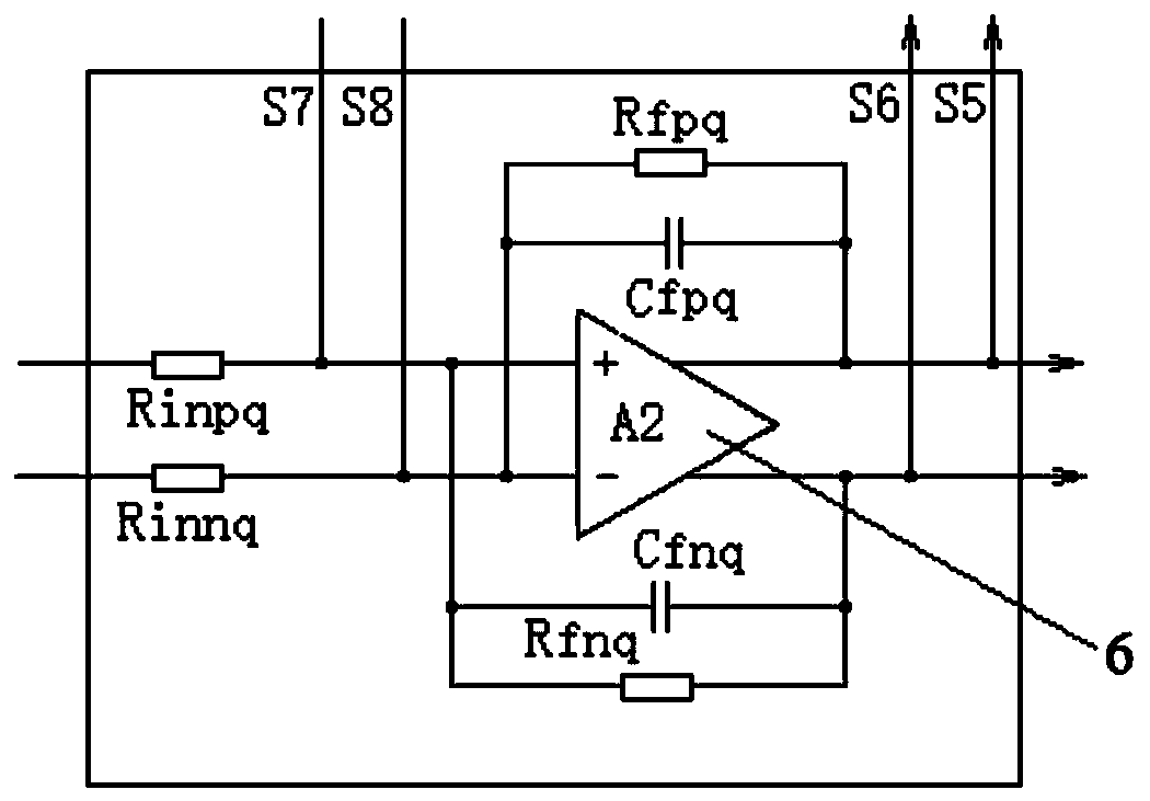
[0021] Embodiment 3, the implementation of imaginary part active filter
[0022] Such as image 3 As shown, described imaginary part active filter 4 is made up of second operational amplifier 6, resistance Rinpq, resistance Rinnq, resistance Rfpq, resistance Rfnq, electric capacity Cfpq and electric capacity Cfnq; Wherein, the noninverting input end of second operational amplifier 6 Connect to one end of resistor Rinpq, resistor Rfnq, and capacitor Cfnq, and connect to the output end (S7) of the switch resistor network; the inverting input end of the second operational amplifier 6 is connected to one end of resistor Rinnq, resistor Rfpq, and capacitor Cfpq , and connected together with the output end (S8) of the switched resistor network; the other end of the resistor Rinpq and the resistor Rinnq are connected with the external input signal; the resistor Rfpq and the capacitor Cfpq are connected in parallel, and connected across the non-inverting output terminal of the second ...
PUM
 Abstract
Description
Claims
Application Information
 - R&D Engineer
- R&D Manager
- IP Professional
- Industry Leading Data Capabilities
- Powerful AI technology
- Patent DNA Extraction
Browse by: Latest US Patents, China's latest patents, Technical Efficacy Thesaurus, Application Domain, Technology Topic, Popular Technical Reports.
© 2024 PatSnap. All rights reserved.Legal|Privacy policy|Modern Slavery Act Transparency Statement|Sitemap|About US| Contact US: help@patsnap.com