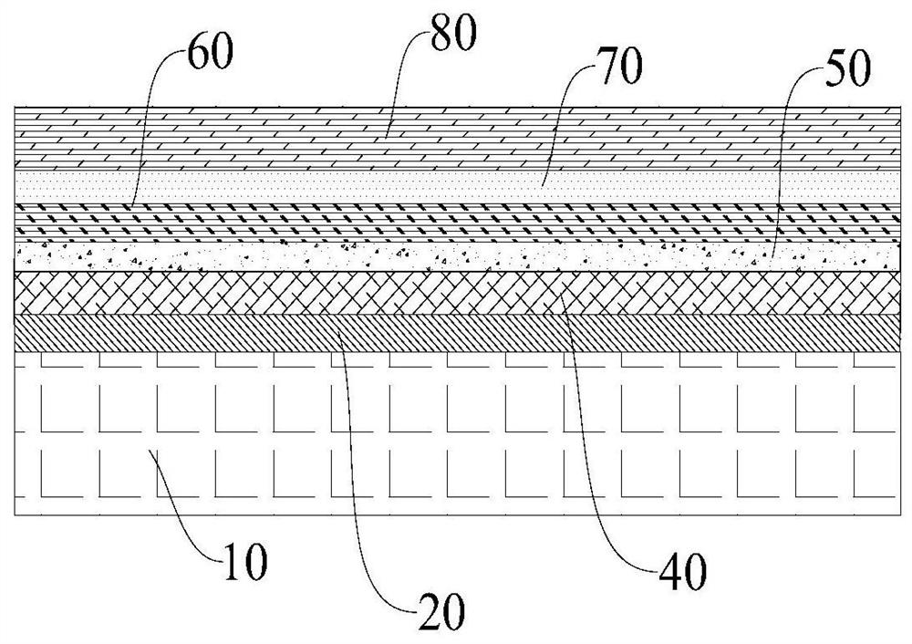
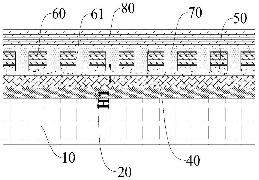
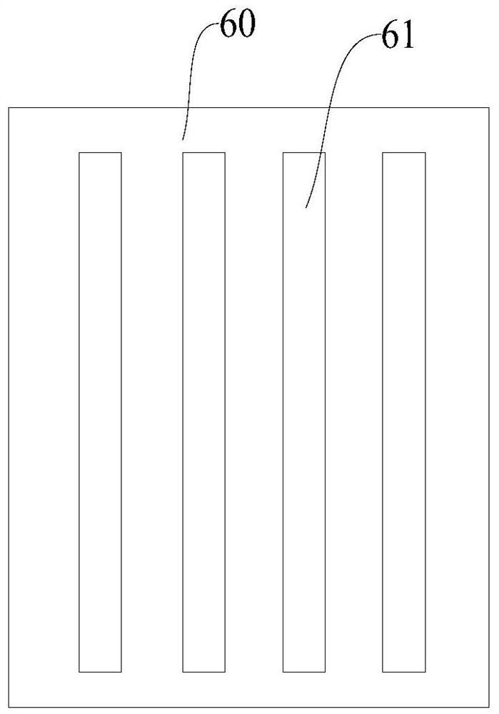
Thin film solar cell and its preparation method
A solar cell and thin-film technology, applied in the field of solar cells, can solve the problems of increased product cost, double-sided thin-film solar cells to be deepened, low energy conversion efficiency of solar cells, etc.
- Summary
- Abstract
- Description
- Claims
- Application Information
AI Technical Summary
Problems solved by technology
Method used
Image
Examples
Embodiment 1
[0061] Test sample: Spiro-OMeTAD hole transport layers with different thicknesses are sequentially formed on a glass transparent substrate to obtain a test sample.
[0062] Test method: Test the light absorption properties of the above test samples under AM1.5G conditions, see the test results and AM1.5G spectral irradiance distribution Figure 9 .
[0063] Figure 9 The spectral irradiance distribution of AM1.5G and the absorption properties of the Spiro-OMeTAD hole transport layer as a function of wavelength and thickness are shown. exist Figure 9 It can be seen that Spiro-OMeTAD, which is a hole transport layer, has a large absorption of light in the wavelength range of 300-400 nm. While this is no problem for single-sided cells (light irradiation on the front side only), in the case of light irradiation on the back side (bifacial cells), although light incidence from both sides has a larger current gain, the There is still some optical loss. Since the light absorptio...
Embodiment 2
[0065] Test sample: The test sample is a plurality of solar cells, the solar cells include a glass transparent substrate, an electron transport layer (titanium dioxide, thickness of 40nm), a perovskite light absorption layer (thickness of 500nm), a hole transport layer ( Spiro-OMeTAD, thickness of 150nm), encapsulation layer and backsheet (glass), the thickness of hole transport layer in multiple solar cells is different, respectively 0nm (ie, does not include hole transport layer), 25nm, 50nm, 75nm , 100nm, 150nm and 200nm.
[0066] Test method: simulate and calculate the photo-generated current density Jph of the above-mentioned multiple solar cells according to the conventional basic logic method in the art.
[0067] Figure 10 The resulting graph of the photogenerated current density Jph as a function of the thickness of the hole transport layer (spiro-OMeTAD) is shown. In this example, in order to analyze the only effect of the thickness of the hole transport layer on t...
Embodiment 3
[0069] Test sample: ITO transparent electrode (thickness is 500nm), electron transport layer (titanium dioxide, thickness is 40nm), perovskite light absorbing layer (thickness is 500nm), hole transport layer (Spiro- OMeTAD with a thickness of 150nm) and an entire metal electrode (silver), using a laser to form openings in the entire metal electrode and the entire hole transport layer, the thickness of the hole transport layer at the bottom of the opening is 0.1nm or 50nm, and then formed Encapsulation layer and glass backplane to obtain test samples, the structure diagram can refer to figure 2 . A series of solar cells with different opening area ratios were fabricated by the above method.
[0070] Test method: simulate and calculate the resistance power loss and absolute efficiency gain of the above series of solar cells according to the conventional basic logic method in the art.
[0071] Figure 11 The resulting plot of resistive power loss as a function of the fraction...
PUM
| Property | Measurement | Unit |
|---|---|---|
| thickness | aaaaa | aaaaa |
| thickness | aaaaa | aaaaa |
| thickness | aaaaa | aaaaa |
Abstract
Description
Claims
Application Information
 - R&D
- Intellectual Property
- Life Sciences
- Materials
- Tech Scout
- Unparalleled Data Quality
- Higher Quality Content
- 60% Fewer Hallucinations
Browse by: Latest US Patents, China's latest patents, Technical Efficacy Thesaurus, Application Domain, Technology Topic, Popular Technical Reports.
© 2025 PatSnap. All rights reserved.Legal|Privacy policy|Modern Slavery Act Transparency Statement|Sitemap|About US| Contact US: help@patsnap.com


