Metal mask forming method for wafer dry etching process

A technology of metal mask and dry etching, which is applied in the field of metal mask formation and wafer technology to achieve the effect of widening the thickness range

Inactive Publication Date: 2019-05-03
BEIJING RES INST OF TELEMETRY +1
View PDF13 Cites 4 Cited by
  • Summary
  • Abstract
  • Description
  • Claims
  • Application Information

AI Technical Summary

Problems solved by technology

[0005] The technical problem solved by the present invention is: to overcome the deficiencies of the prior art, to provide a metal mask forming method for wafer dry etching process, to make up for the difficulty in preparing thick metal masks by physical methods and the difficulty in controlling the thickness by corrosion methods. lack of metal precision

Method used


Image

  • Metal mask forming method for wafer dry etching process
  • Metal mask forming method for wafer dry etching process
  • Metal mask forming method for wafer dry etching process

Examples


Embodiment

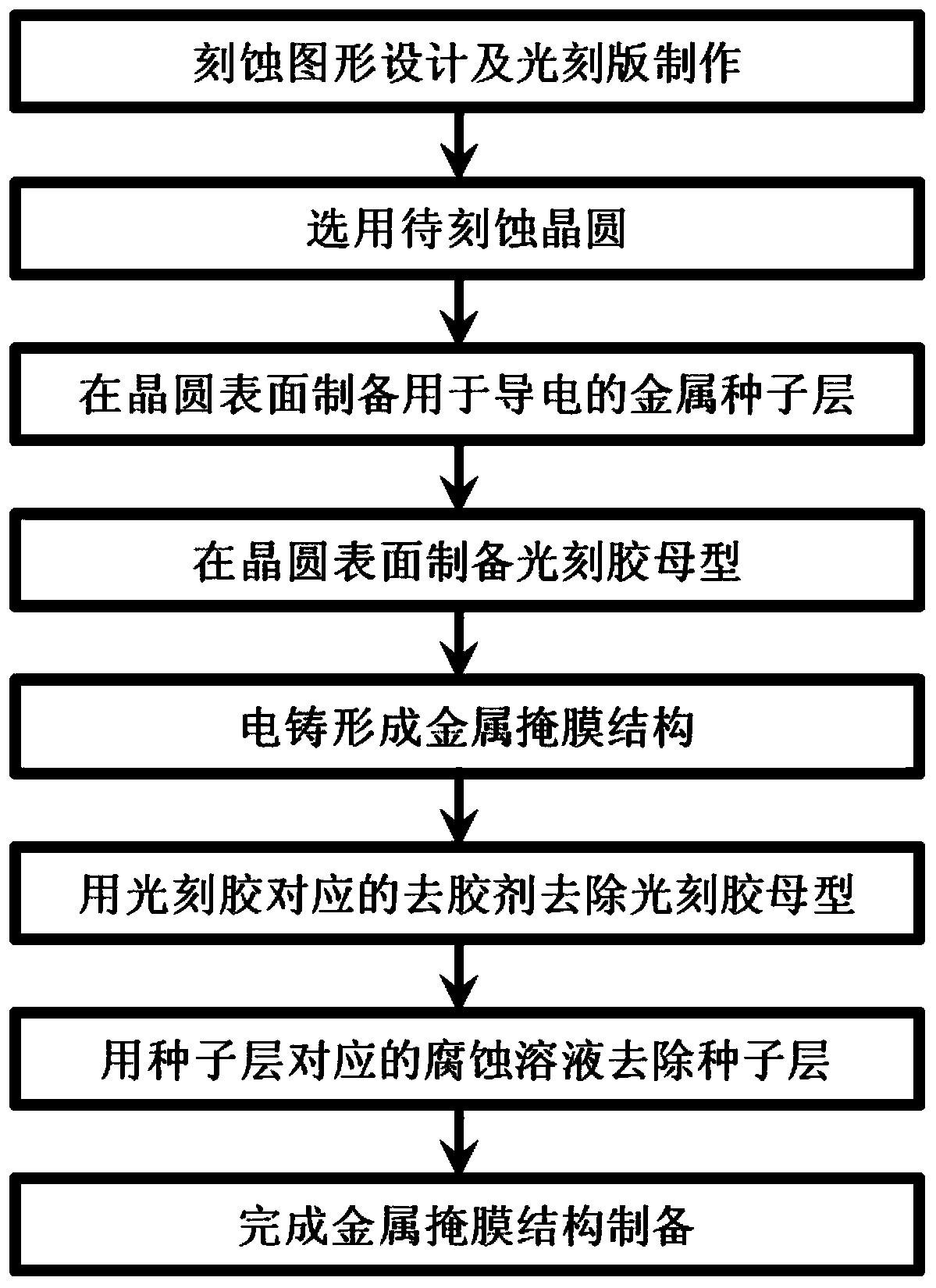
[0046] (1) According to the requirements of the etching structure, the mask structure photolithography layout is designed and processed to form a photolithography plate for etching wafer patterns.

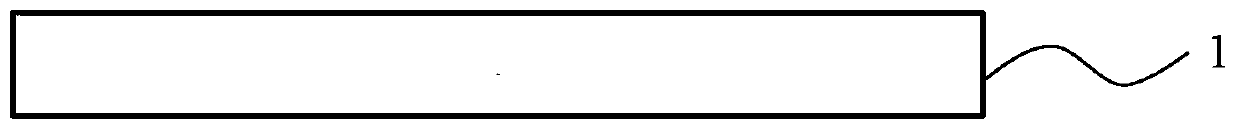
[0047] (2) Select a wafer 1 for etching, such as single crystal silicon carbide, quartz, gallium lanthanum silicate, glass, etc., which can be etched by using a metal mask. Such as figure 2 shown.

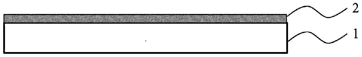
[0048] (3) Decontamination and cleaning are performed on the selected wafers. Wet solution cleaning can be used, such as acetone, ethanol and other organic solvents for ultrasonic cleaning for 10 to 20 minutes, and concentrated H can also be used according to different requirements or wafer materials. 2 SO 4 with H 2 o 2 Configure the cleaning solution according to the volume ratio, heat and boil for 10-20 minutes, and then wash with water, blow the residual water stains on the surface of the wafer with nitrogen, and put it in a drying oven for drying treatment at a temperature ab...


PUM

PropertyMeasurementUnit
thicknessaaaaaaaaaa
thicknessaaaaaaaaaa
thicknessaaaaaaaaaa

Abstract

The invention discloses a metal mask forming method for a wafer dry etching process. The method is particularly suitable for a monocrystal silicon carbide or quartz wafer etching process, and comprises preparing a metal seed layer on a wafer surface; forming a photoresist model by a photoresist; and preparing an electroformed metal mask by an electroforming method. The thickness of the prepared metal mask is not limited, and can range from hundreds of nanometers to hundreds of micrometers. Thus, the method greatly expands the thickness range of the metal mask, avoids the poor lateral etching precision caused by the wet etching process of the metal mask, and in particular, can improve the pattern accuracy of metal masks for a thick etching process.

Description

technical field [0001] The invention relates to a method for forming a micro-process of a wafer etching mask, in particular to a method for forming a metal mask for a wafer dry etching process, which is suitable for wafers that can be processed by deep etching using a metal mask. Round process, such as silicon carbide or quartz wafer, etc. Background technique [0002] Dry etching is a vacuum plasma processing technology gradually developed along with the progress of semiconductor wafer micro process technology. Dry etching has been developed into a commonly used micro-processing method. It mainly uses the difference in the physical or chemical effects of vacuum plasma particles on different materials to bombard the surface of the wafer with a mask, so as to etch the wafer material. And form the purpose of a specific structure. Dry etching was mainly aimed at the processing of silicon wafers and metal thin film structures at the beginning, and was used for the preparation ...

Claims


Application Information

Patent Timeline
Patent Type & Authority Applications(China)
IPC IPC(8): H01L21/308H01L21/027C25D1/10
Inventor 赵广宏许姣曹正威尹玉刚金小锋
Owner BEIJING RES INST OF TELEMETRY
Why Eureka
Try Eureka