


Quick Research
Generate reliable direction feasibility study reports for your R&D in just a few steps.

Technical Q&A
Discover and master advanced knowledge NOW. Basics, ideas, possibilities, all at once.

Find Solutions
As an expert in R&D theories, this can generate solutions to your technical problems instantly.

Evaluate Feasibility
Analyze your overall solution with one click, know your potential R&D risks in advance.

Monitor Landscape
Get weekly tech updates, stay abreast of the latest tech innovations and key insights.
Solid solution nanowire as well as preparation method and application thereof
A nanowire and solid solution technology, which is applied in nanotechnology, nanotechnology, nanotechnology for materials and surface science, etc. Effect
- Summary
- Abstract
- Description
- Claims
- Application Information
AI Technical Summary
Problems solved by technology
Method used
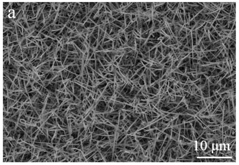
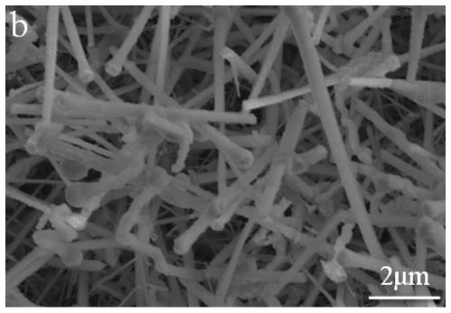
Image

Examples
Embodiment 1
[0081] This embodiment prepares solid solution nanowires according to the following method:
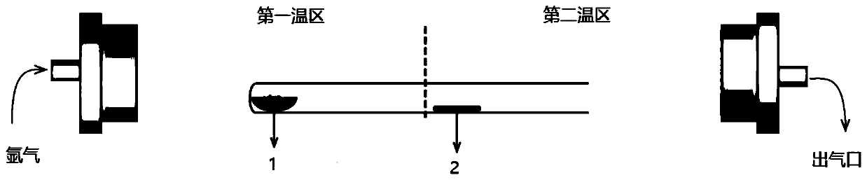
[0082] (1) Cut the silicon wafer into 1×1 cm slices, use acetone, isopropanol and absolute ethanol as solvents to ultrasonically clean the silicon wafers for 15 minutes, and dry them with nitrogen to obtain pretreated silicon wafers. Carry out ion sputtering covering gold film (i.e. spraying gold) with ion sputtering instrument on the silicon chip of above-mentioned pretreatment with the electric current of 9mA, the time of ion sputtering is 90s, obtains the substrate that covers gold, described covered gold The substrate is placed in the reactor and evacuated by a vacuum pump until the pressure in the quartz tube reactor is 1Pa, then argon gas with a flow rate of 50 sccm is introduced, and annealing is performed at 450°C for 30 minutes, and the annealed substrate is obtained after natural cooling;
[0083] (2) The mixture of InP and ZnSe (in the mixture, the molar percentage of InP i...
Embodiment 2
[0095] This embodiment prepares solid solution nanowires according to the following method:
[0096] (1) Cut the silicon wafer into 1×1 cm slices, use acetone, isopropanol and absolute ethanol as solvents to ultrasonically clean the silicon wafers for 15 minutes, and dry them with nitrogen to obtain pretreated silicon wafers. Carry out ion sputtering covering gold film (i.e. spraying gold) with the electric current of 8mA on the silicon chip of above-mentioned pretreatment, the time of ion sputtering is 120s, obtains the substrate that covers gold, the described covered gold Place the substrate in the reactor and evacuate it with a vacuum pump until the pressure in the quartz tube reactor is 0.9Pa, then flow argon gas with a flow rate of 40sccm, anneal at 420°C for 40min, and cool naturally to obtain an annealed substrate ;
[0097] (2) The mixture of InP and ZnSe (in the mixture, the molar percentage of InP is 50%) is placed at the end of the sealed end of the quartz tube wi...
Embodiment 3
[0101] This embodiment prepares solid solution nanowires according to the following method:
[0102] (1) Cut the silicon wafer into 1×1 cm slices, use acetone, isopropanol and absolute ethanol as solvents to ultrasonically clean the silicon wafers for 15 minutes, and dry them with nitrogen to obtain pretreated silicon wafers. Carry out ion sputtering and cover gold film (i.e. spray gold) with ion sputtering instrument on the silicon chip of above-mentioned pretreatment with the electric current of 10mA, the time of ion sputtering is 60s, obtains the substrate that covers gold, the described cover gold Place the substrate in the reactor and evacuate it with a vacuum pump until the pressure in the quartz tube reactor is 0.85Pa, then pass in argon gas with a flow rate of 60sccm, and anneal at 480°C for 20 minutes. After natural cooling, the annealed substrate is obtained. ;
[0103] (2) The mixture of InP and ZnSe (in the mixture, the molar percentage of InP is 66.7%) is placed ...
PUM
| Property | Measurement | Unit |
|---|---|---|
| diameter | aaaaa | aaaaa |
| length | aaaaa | aaaaa |
| diameter | aaaaa | aaaaa |
Abstract
Description
Claims
Application Information
 - R&D Engineer
- R&D Manager
- IP Professional
- Industry Leading Data Capabilities
- Powerful AI technology
- Patent DNA Extraction
Browse by: Latest US Patents, China's latest patents, Technical Efficacy Thesaurus, Application Domain, Technology Topic, Popular Technical Reports.
© 2024 PatSnap. All rights reserved.Legal|Privacy policy|Modern Slavery Act Transparency Statement|Sitemap|About US| Contact US: help@patsnap.com