Eureka AIR delivers breakthrough ideas for toughest innovation challenges, trusted by R&D personnel around the world.

Thinning method of silicon carbide wafer

A silicon carbide crystal and silicon carbide technology, which is used in grinding machine parts, fine working devices, and workpiece feed motion control, etc., can solve wafer fragmentation, wafer thinning, low yield, and grinding wheel wear higher problem

Inactive Publication Date: 2019-04-23
厦门芯光润泽科技有限公司
View PDF8 Cites 1 Cited by
  • Summary
  • Abstract
  • Description
  • Claims
  • Application Information

AI Technical Summary

Problems solved by technology

However, since silicon carbide is a hard, brittle and difficult-to-machine material, the wear ratio of the grinding wheel is extremely high
[0004] In addition, as the size of the wafer increases, when the wafer is thinned below a certain thickness, the stress and damage of the silicon carbide wafer are severe, and the wafer is easily broken, resulting in an extremely low yield of wafer thinning

Method used


Image

  • Thinning method of silicon carbide wafer
  • Thinning method of silicon carbide wafer
  • Thinning method of silicon carbide wafer

Examples


Embodiment

[0054] Backside thinning of 6-inch SiC wafers.

[0055] Confirm that the initial thickness of the 6-inch (about 150mm in diameter) silicon carbide wafer is 350 μm, the second target thickness is about 120 μm, and the thickness to be thinned is about 230 μm.

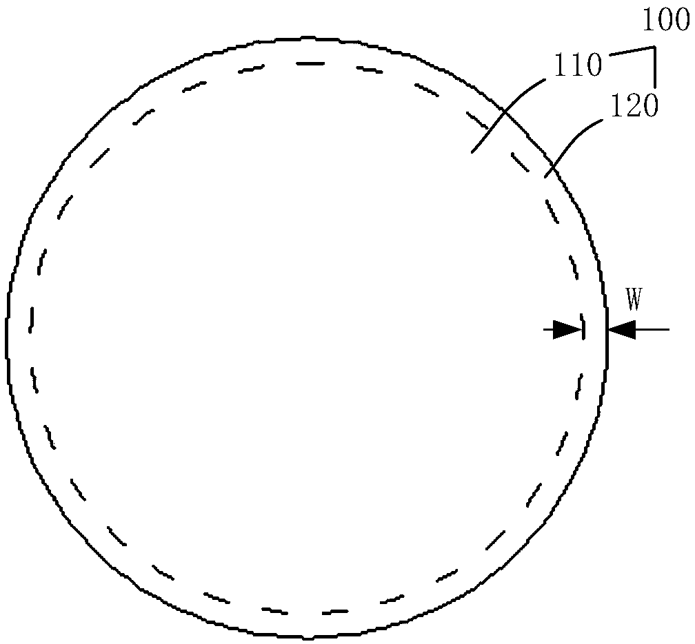
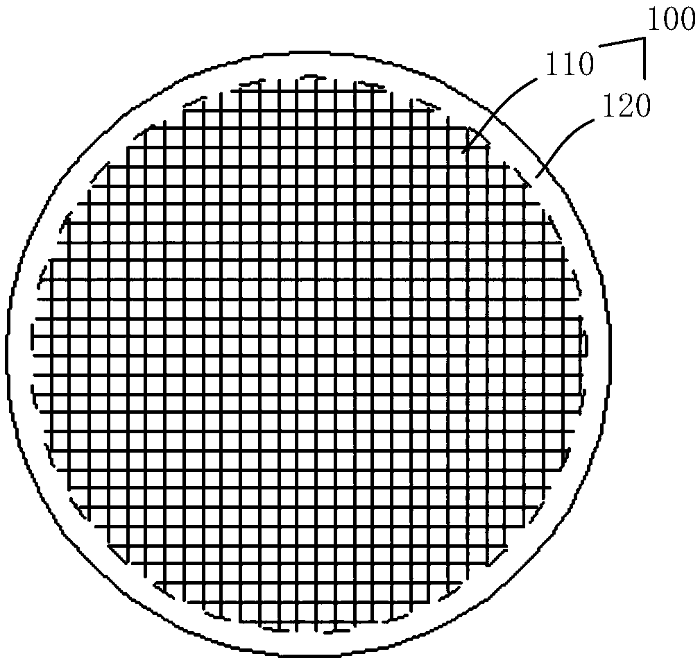
[0056] Such as figure 1 As shown, a security ring area 120 and a laser pre-processing area 110 are provided on the back side of the silicon carbide wafer 100 . Wherein, the truncated width W of the laser pre-processing region 110 is 4mm (accounting for about 2.6% of the diameter).

[0057] Place the wafer on the laser scanning workbench, and set the laser scanning process parameters as follows:

[0058] Adjust the focus, the first laser power is 0.55watt, the repetition frequency is 15KHz, the scanning speed is 30mm / s, and the auxiliary air pressure is 0.6Mpa;

[0059] Adjust the focus, the second laser power is 0.33watt, the repetition frequency is 25KHz, the scanning speed is 40mm / s, and the auxiliary air pressure is...


PUM

PropertyMeasurementUnit
wavelengthaaaaaaaaaa
thicknessaaaaaaaaaa
diameteraaaaaaaaaa

Abstract

The invention discloses a thinning method of a silicon carbide wafer. The method comprises the steps that the back face of the silicon carbide wafer is divided into the safety ring area and the laserpre-processing area; the laser pre-processing area is a circular area with the area smaller than the area of the silicon carbide wafer back face, and the safety ring area surrounds the edge ring areaof the laser pre-processing area; laser scanning is carried out on the laser pre-processing area, and a laser groove is formed; the position, with the laser groove, of the back face of the silicon carbide wafer is roughly ground until the position is ground to the first target thickness; the silicon carbide wafer back with the first target thickness is subjected to fine grinding until the back face is ground to the second target thickness; and according to the thinning method of the silicon carbide wafer, the fragment problem in the thinning process of the silicon carbide wafer back face is solved, the thinned surface and the subsurface damage of the silicon carbide wafer back face can be improved, the consumable amount of a grinding wheel used during grinding can be reduced, and machiningcost is reduced.

Description

technical field [0001] The invention relates to the field of semiconductor technology, in particular to a method for thinning a silicon carbide wafer. Background technique [0002] Silicon carbide power devices are suitable for extreme working environments such as high temperature, high voltage and high radiation due to their excellent performance. However, silicon carbide devices still generate a lot of heat when working in high-power and extreme environments. By reducing the thermal resistance of the device substrate part, the power loss of the device can be effectively reduced and its heat dissipation can be improved, which plays an important role in the overall performance and life of the device. critical use. [0003] At present, the mainstream technology for preparing large-size ultra-thin silicon carbide in the industry is to use a wafer back thinner to grind and thin the back of the silicon carbide wafer, which can effectively reduce the thermal resistance of the su...

Claims


Application Information

Patent Timeline
Patent Type & Authority Applications(China)
IPC IPC(8): B24B7/22B24B49/12B28D5/00
Inventor 卓廷厚罗求发柴雅玲
Owner 厦门芯光润泽科技有限公司
Why Eureka
Eureka Blog
Learn More