High-thermal-conductivity electronic package composite material and preparation method thereof
A technology of electronic packaging and composite materials, which is applied in nanotechnology, circuits, electrical components, etc. for materials and surface science. Effect of electromigration failure time
- Summary
- Abstract
- Description
- Claims
- Application Information
AI Technical Summary
Problems solved by technology
Method used
Image

Examples
Embodiment 1
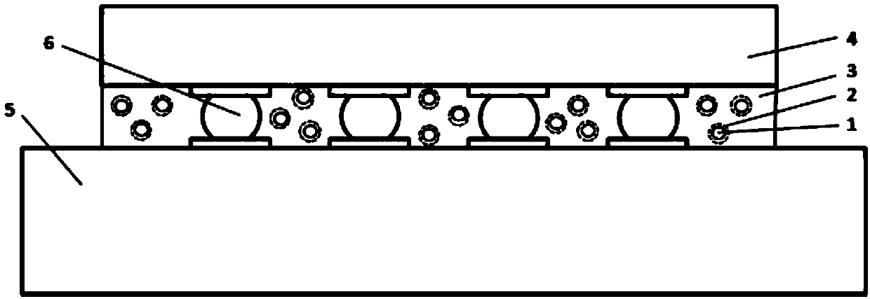
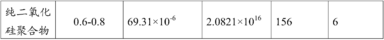
[0037] The high thermal conductivity electronic packaging composite material provided by the invention is used on the packaging filling of microelectronic chips, such as figure 1 As shown, the outer surface of the nano-copper particles 1 is covered with a silicon dioxide layer 2; the silicon dioxide layer 2 is used as an insulating layer, and its thickness is 10-100 nm; the particle size of the nano-copper particles is 50-500 nm. The nano-copper particles wrapped with the silicon dioxide layer 2 are mixed with the polymer 3 to form a high thermal conductivity electronic packaging composite material; wherein, the volume ratio of the insulating nano-particles to the polymer is 0.1-0.3. Polymers include epoxy, acrylate or phenolic resins.
[0038] Fill the electronic packaging compound material with high thermal conductivity between the chip 4 and the substrate 5. The micro bump 6 is also included between the chip 4 and the substrate 5. The micro bump 6 is the I / O connection betw...
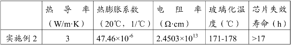
Embodiment 2
[0041] Step 1: Weigh 2mmol copper oxalate and dissolve it in 25ml N,N-dimethylformamide solution;
[0042] Step 2: Add 1mmol polyvinylpolypyrrolidone and 1.3mmol sodium borohydride to the solution in step 1;
[0043] Step 3: After stirring for five minutes, the above mixture was heated to 85°C and kept for 3 minutes, and then filtered to obtain an orange precipitate, which is called filter residue A, and the filter residue A was washed several times with alcohol to obtain intermediate product A;
[0044]Step 4: Dissolving and dispersing the intermediate product A obtained in Step 3 in a mixed solution of 60ml of water and 40ml of ethanol to obtain a mixed solution;
[0045] Step 5: Add 1 mL of concentrated ammonia water to the mixed solution in Step 4, and then add 0.24 mmol of ethyl orthosilicate; wherein, the concentration of ammonia water is 28% by mass;
[0046] Step 6: After stirring at room temperature for 6 hours, filter to obtain filter residue B, wash filter residue ...
Embodiment 3
[0054] Step 1: Weigh 3mmol copper oxalate and dissolve it in 50ml N,N-dimethylformamide solution;
[0055] Step 2: Add 1.6mmol polyvinylpolypyrrolidone and 1.8mmol sodium borohydride to the step 1 solution;
[0056] Step 3: After stirring for five minutes, the above mixture was heated to 90°C and kept for 4 minutes, and then filtered to obtain an orange precipitate, which is called filter residue A, and the filter residue A was washed several times with alcohol to obtain intermediate product A;
[0057] Step 4: Dissolving and dispersing the intermediate product A obtained in Step 3 in a mixed solution of 75ml of water and 75ml of ethanol to obtain a mixed solution;
[0058] Step 5: Add 3 mL of concentrated ammonia water to the mixed solution in Step 4, and then add 0.3 mmol of tetraethyl orthosilicate; wherein, the concentration of ammonia water is 26% by mass;
[0059] Step 6: After stirring at room temperature for 7 hours, filter to obtain filter residue B, wash filter resi...
PUM
| Property | Measurement | Unit |
|---|---|---|
| Thickness | aaaaa | aaaaa |
| Particle size | aaaaa | aaaaa |
| Concentration | aaaaa | aaaaa |
Abstract
Description
Claims
Application Information
 - R&D
- Intellectual Property
- Life Sciences
- Materials
- Tech Scout
- Unparalleled Data Quality
- Higher Quality Content
- 60% Fewer Hallucinations
Browse by: Latest US Patents, China's latest patents, Technical Efficacy Thesaurus, Application Domain, Technology Topic, Popular Technical Reports.
© 2025 PatSnap. All rights reserved.Legal|Privacy policy|Modern Slavery Act Transparency Statement|Sitemap|About US| Contact US: help@patsnap.com