Semiconductor device and method of forming the same

A semiconductor and device technology, which is applied in the field of semiconductor devices and their formation, can solve problems such as performance improvement, and achieve the effects of improving performance, avoiding excessive distance, and avoiding excessive resistance

Active Publication Date: 2022-04-15
SEMICON MFG INT (SHANGHAI) CORP +1
View PDF0 Cites 0 Cited by
  • Summary
  • Abstract
  • Description
  • Claims
  • Application Information

AI Technical Summary

Problems solved by technology

[0004] However, the performance of semiconductor devices composed of fin field effect transistors in the prior art still needs to be improved

Method used


Image

  • Semiconductor device and method of forming the same
  • Semiconductor device and method of forming the same
  • Semiconductor device and method of forming the same

Examples


Embodiment Construction

[0029] As mentioned in the background, semiconductor devices formed in the prior art have poor performance.

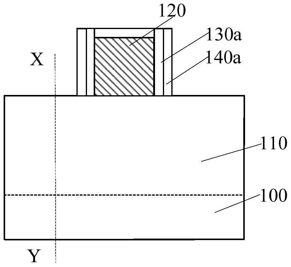
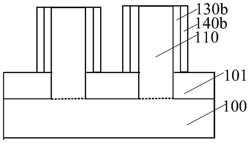
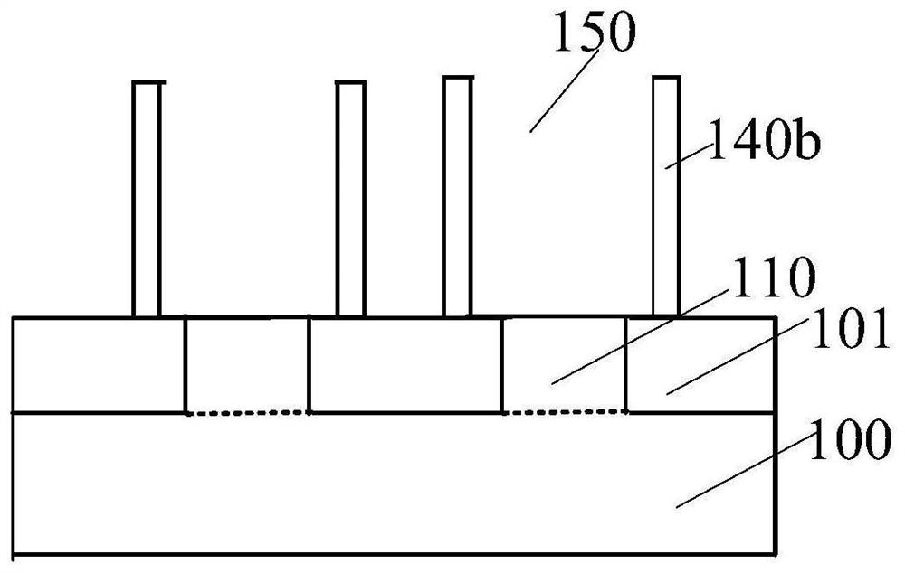
[0030] Figure 1 to Figure 3 It is a structural schematic diagram of the formation process of a semiconductor device.

[0031] combined reference figure 1 and figure 2 , figure 2 along figure 1 The cross-sectional view of cutting line X-Y in the middle provides a semiconductor substrate 100 with several fins 110 and an isolation layer 101 covering part of the sidewalls of the fins 110 on the semiconductor substrate 100, and the exposed fins of the isolation layer 101 include replacement regions Form the gate structure 120 across the fin 110 on the semiconductor substrate 100 and the isolation layer 101, and the fin replacement regions are respectively located on both sides of the gate structure 120; during the process of forming the first fin spacer 130b, the first Gate spacer 130a, the first fin sidewall 130b is located on the sidewall of the replacement regio...


PUM

PropertyMeasurementUnit
thicknessaaaaaaaaaa
thicknessaaaaaaaaaa

Abstract

A semiconductor device and a method for forming the same, wherein the method includes: providing a semiconductor substrate with a plurality of fins and an isolation layer covering sidewalls of the fins on the semiconductor substrate; forming a gate structure on the semiconductor substrate and the isolation layer, The gate structure spans the fin and covers part of the top surface and part of the sidewall surface of the fin, and the fins on both sides of the gate structure have replacement regions; using a selective epitaxial growth process on the sidewalls of the fin replacement regions Forming a sacrificial layer on the surface of the isolation layer; forming a fin sidewall on the surface of the isolation layer on the sidewall of the sacrificial layer, and forming a gap sidewall on the sidewall of the gate structure during the formation of the fin sidewall; removing the gate structure and the gap The replacement area on both sides of the sidewall and the sacrificial layer form a groove in the fin, and the sidewalls on both sides of the groove in the width direction of the fin respectively expose the fin sidewall; the source is formed in the groove Drain doped layer. The method improves the performance of semiconductor devices.

Description

technical field [0001] The invention relates to the field of semiconductor manufacturing, in particular to a semiconductor device and a forming method thereof. Background technique [0002] MOS (Metal-Oxide-Semiconductor) transistors are one of the most important components in modern integrated circuits. The basic structure of the MOS transistor includes: a semiconductor substrate; a gate structure located on the surface of the semiconductor substrate, and the gate structure includes: a gate dielectric layer located on the surface of the semiconductor substrate and a gate electrode layer located on the surface of the gate dielectric layer; The source and drain doped regions in the semiconductor substrate on both sides of the pole structure. [0003] With the development of semiconductor technology, the ability of the traditional planar MOS transistor to control the channel current becomes weaker, resulting in serious leakage current. Fin Field Effect Transistor (Fin FET) i...

Claims


Application Information

Patent Timeline
Patent Type & Authority Patents(China)
IPC IPC(8): H01L21/336H01L29/78
CPCH01L29/66795H01L29/785
Inventor 周飞
Owner SEMICON MFG INT (SHANGHAI) CORP
Why Eureka
Try Eureka