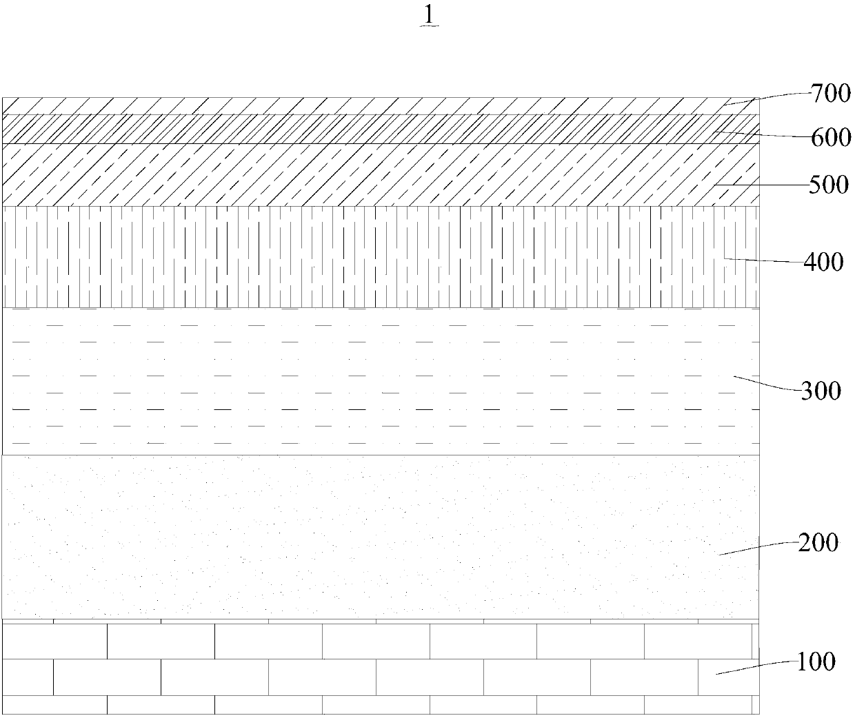
Disc-type laser device
A laser device, disc type technology, applied in the field of optical communication, can solve the problems of large size, disadvantageous silicon-based optical chips, increase the coupling cost of laser and silicon chips, etc., and achieve the effects of small size, excellent luminous intensity and threshold value
- Summary
- Abstract
- Description
- Claims
- Application Information
AI Technical Summary
Problems solved by technology
Method used
Image
Examples
Embodiment 1
[0069] A disc type laser device, comprising a silicon substrate, an InGaAs / GaAs superlattice defect suppression layer formed on the silicon substrate, a GaAs buffer layer formed on the defect suppression layer, and a GaAs buffer layer formed on the GaAs buffer layer al 0.6 Ga 0.4 As sacrificial layer, formed on the Al 0.6 Ga 0.4 One active layer on As sacrificial layer, Al formed on three active layers 0.4 Ga 0.6 As layer and formed on Al 0.4 Ga 0.6 GaAs layer on top of the As layer.
[0070] As mentioned above, the active layer consists of In 0.15 Ga 0.85 As (InGaAs) quantum wells and confined in In 0.15 Ga 0.85 InAs quantum dots in As (indium gallium arsenide) quantum wells.
[0071] The thickness of the above-mentioned silicon substrate is 0.7um, the thickness of the defect suppression layer is 3um, the thickness of the GaAs buffer layer is 2.2um, the Al x Ga 1-x The thickness of As sacrificial layer is 1.3um, the thickness of one active layer is 350nm, Al 0.4...
Embodiment 2
[0078] A disc type laser device, comprising a silicon substrate, an InGaAs / GaAs superlattice defect suppression layer formed on the silicon substrate, a GaAs buffer layer formed on the defect suppression layer, and a GaAs buffer layer formed on the GaAs buffer layer al 0.6 Ga 0.4 As sacrificial layer, formed on the Al 0.6 Ga 0.4 Two active layers on As sacrificial layer, Al formed on three active layers 0.4 Ga 0.6 As layer and formed on Al 0.4 Ga 0.6 GaAs layer on top of the As layer.
[0079] As mentioned above, the active layer consists of In 0.15 Ga 0.85 As (InGaAs) quantum wells and confined in In 0.15 Ga 0.85 InAs quantum dots in As (indium gallium arsenide) quantum wells.
[0080] The thickness of the above-mentioned silicon substrate is 0.8um, the thickness of the defect suppression layer is 3.2um, the thickness of the GaAs buffer layer is 2.4um, the Al x Ga 1-x The thickness of the As sacrificial layer is 1.5um, the thickness of the two active layers is 355n...
Embodiment 3
[0083] A disc type laser device, comprising a silicon substrate, an InGaAs / GaAs superlattice defect suppression layer formed on the silicon substrate, a GaAs buffer layer formed on the defect suppression layer, and a GaAs buffer layer formed on the GaAs buffer layer al 0.6 Ga 0.4 As sacrificial layer, formed on the Al 0.6 Ga 0.4 Three active layers on As sacrificial layer, Al formed on three active layers 0.4 Ga 0.6 As layer and formed on Al 0.4 Ga 0.6 GaAs layer on top of the As layer.
[0084] As mentioned above, the active layer consists of In 0.15 Ga 0.85 As (InGaAs) quantum wells and confined in In 0.15 Ga 0.85 InAs quantum dots in As (indium gallium arsenide) quantum wells.
[0085] The thickness of the above-mentioned silicon substrate is 0.9um, the thickness of the defect suppression layer is 3.5um, the thickness of the GaAs buffer layer is 2.5um, the Al x Ga 1-x The thickness of the As sacrificial layer is 1.6um, the thickness of the three active layers i...
PUM
 Abstract
Description
Claims
Application Information
 - R&D Engineer
- R&D Manager
- IP Professional
- Industry Leading Data Capabilities
- Powerful AI technology
- Patent DNA Extraction
Browse by: Latest US Patents, China's latest patents, Technical Efficacy Thesaurus, Application Domain, Technology Topic, Popular Technical Reports.
© 2024 PatSnap. All rights reserved.Legal|Privacy policy|Modern Slavery Act Transparency Statement|Sitemap|About US| Contact US: help@patsnap.com


