Ceramic capacitor for reducing parasitic inductance

A ceramic capacitor and parasitic inductance technology, applied in the direction of multilayer capacitors, fixed capacitor electrodes, fixed capacitor dielectrics, etc., can solve problems such as large parasitic inductance, reduce the existence of internal parasitic inductance, reduce parasitic inductance, and reduce the transmission path. Effect

Inactive Publication Date: 2019-04-05
ZHENGZHOU YUNHAI INFORMATION TECH CO LTD
View PDF4 Cites 0 Cited by
  • Summary
  • Abstract
  • Description
  • Claims
  • Application Information

AI Technical Summary

Problems solved by technology

[0003] The purpose of the present invention is to provide a ceramic capacitor with reduced parasitic inductance, which is used to solve the technical problem of a large amount of parasitic inductance inside the ceramic capacitor

Method used


Image

  • Ceramic capacitor for reducing parasitic inductance
  • Ceramic capacitor for reducing parasitic inductance
  • Ceramic capacitor for reducing parasitic inductance

Examples


Embodiment Construction

[0023] In order to clearly illustrate the technical characteristics of this solution, the following specific implementation methods are combined with the attached Figure 1 to 6 , To elaborate on the present invention. It should be noted that the components illustrated in the drawings are not necessarily drawn to scale. The present invention omits descriptions of well-known components and well-known technologies to avoid unnecessarily limiting the present invention.

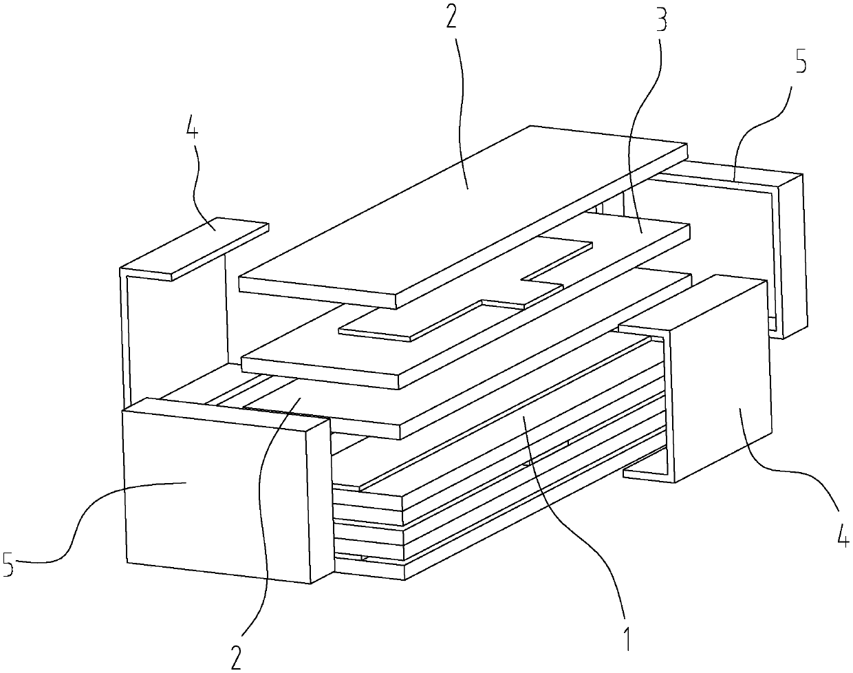
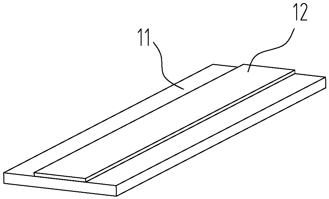
[0024] A ceramic capacitor for reducing parasitic inductance, comprising a first chip 1, a ceramic dielectric sheet 2, a second chip 3, a grounded external electrode plate 4 and a signal external electrode plate 5; the first chip 1 includes a first ceramic substrate 11 and The first internal electrode 12 is provided on the surface of the first ceramic substrate 11, and the first internal electrode 12 extends laterally to the left and right sides of the first ceramic substrate 11. The second chip 3 includes a secon...


PUM


Abstract

A ceramic capacitor for reducing parasitic inductance belongs to the technical field of ceramic capacitors and comprises a first chip, ceramic dielectric thin pieces, a second chip, two grounding external electrode plates and two signal external electrode plates, wherein the first chip comprises a first ceramic substrate and a first inner electrode, the first inner electrode horizontally extends to a left side surface and a right side surface of the first ceramic substrate, the second chip comprises a second ceramic substrate and a second inner electrode, the second inner electrode longitudinally extends to a front side surface and a rear side surface of the second ceramic substrate, the ceramic dielectric thin pieces are sandwiched between the first chip and the second chip and are laminated to form a chip body, the ceramic dielectric thin piece is arranged at each of an upper side and lower side of the chip body, the two grounding external electrode plates are respectively arranged at a front side surface and a rear side surface of the second chip, and the two signal external electrode plates are respectively arranged at a left side surface and a right side surface of the first chip. The ceramic capacitor is used for solving the technical problem that a large amount of parasitic inductance exists in the ceramic capacitor.

Description

Technical field [0001] The invention relates to the technical field of ceramic capacitors, in particular to a ceramic capacitor that reduces parasitic inductance. Background technique [0002] At present, most of the chip multilayer ceramic capacitors used have a two-terminal electrode structure. The structure is that the internal electrodes on the chip sandwich the ceramic dielectric and are alternately stacked in a staggered manner. After high temperature sintering, the two Seal the outer electrode on the end. This kind of ceramic capacitor has a unidirectional transmission due to its internal transmission and a long transmission path, which still has a large amount of parasitic inductance. The existence of parasitic inductance will cause the performance of the ceramic capacitor to decrease. Summary of the invention [0003] The purpose of the present invention is to provide a ceramic capacitor with reduced parasitic inductance, which is used to solve the technical problem of a...

Claims


Application Information

Patent Timeline
Patent Type & Authority Applications(China)
IPC IPC(8): H01G4/30H01G4/12H01G4/005H01G4/232
CPCH01G4/012H01G4/12H01G4/232H01G4/30
Inventor 杨光明
Owner ZHENGZHOU YUNHAI INFORMATION TECH CO LTD
Why Eureka
Try Eureka