Method of forming semiconductor device

A semiconductor and device technology, applied in the field of semiconductor devices and their formation, can solve the problems of poor performance of semiconductor devices, affecting the threshold voltage of semiconductor devices, etc., and achieve the effect of improving device performance and reducing loss

Active Publication Date: 2020-10-09
SEMICON MFG INT (SHANGHAI) CORP +1
View PDF5 Cites 0 Cited by
  • Summary
  • Abstract
  • Description
  • Claims
  • Application Information

AI Technical Summary

Problems solved by technology

[0005] However, the existing methods for forming semiconductor devices easily affect the threshold voltage of the formed semiconductor devices, thus making the formed semiconductor devices poor in performance

Method used


Image

  • Method of forming semiconductor device
  • Method of forming semiconductor device
  • Method of forming semiconductor device

Examples


Embodiment Construction

[0031] As mentioned in the background art, with the increase in density and the reduction in size of semiconductor devices, the electrical performance of semiconductor devices still needs to be improved.

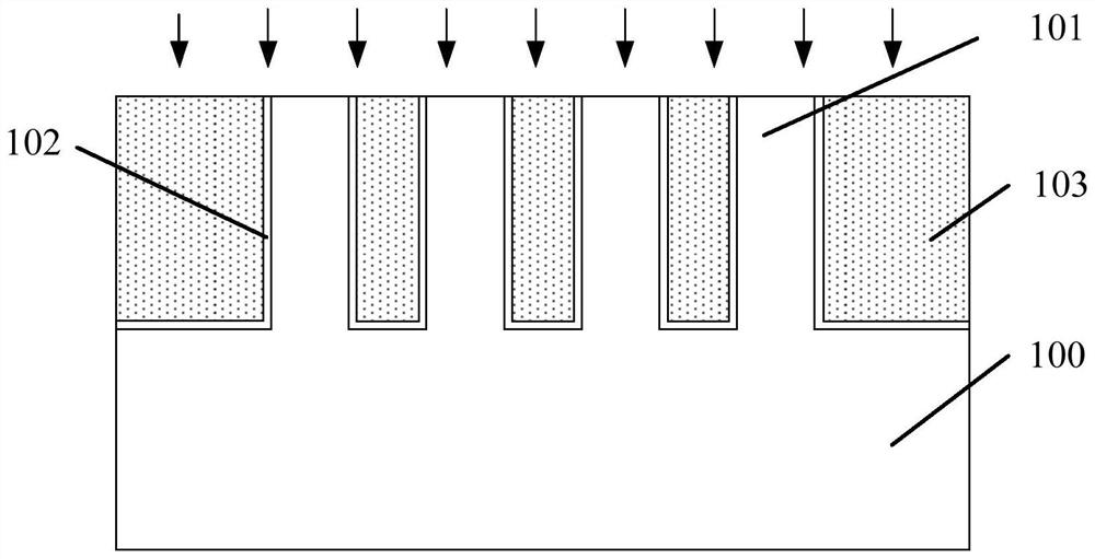
[0032] Since the size of the semiconductor device is smaller, the fin size of the device is also smaller, the capacity for doping ions is also smaller, and the state of doping ions after heat treatment is also more unstable, which affects the performance of the fin transistor device. It is also more obvious, and will be described below in conjunction with the accompanying drawings.

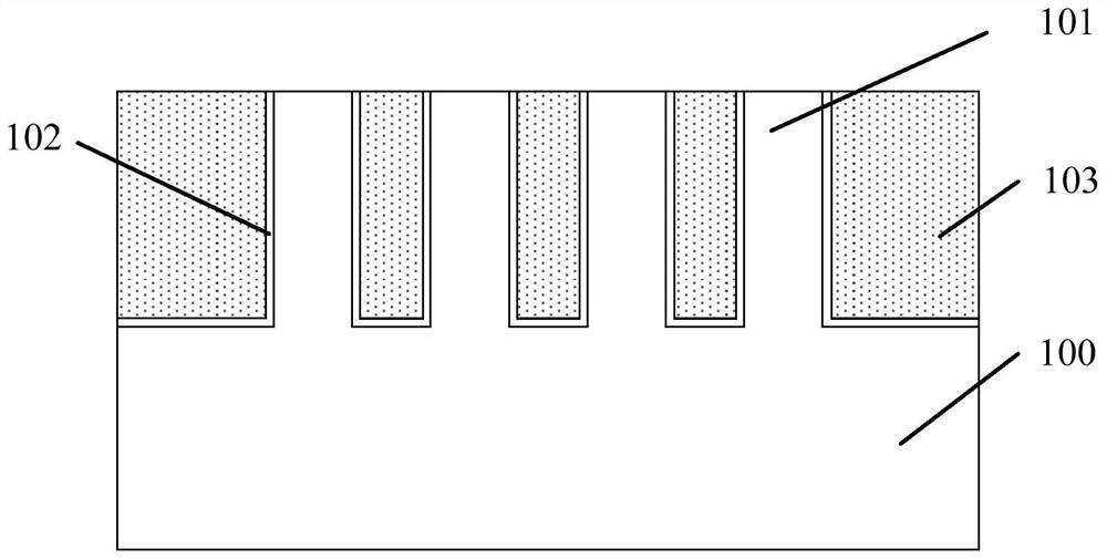
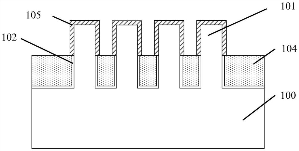
[0033] Figure 1 to Figure 3 It is a schematic cross-sectional structure diagram of the formation process of a semiconductor device.

[0034] Please refer to figure 1 , providing a substrate 100 with a fin 101 on the substrate, forming a protective layer 102 on the fin and the substrate, the protective layer 102 covering the substrate and the sidewall of the fin, exposing the top of the fin, a...


PUM

PropertyMeasurementUnit
thicknessaaaaaaaaaa
thicknessaaaaaaaaaa

Abstract

The present invention provides a method of forming a semiconductor device. The method comprises the steps of: providing a substrate having a fin thereon; forming a dummy gate oxide layer at the side wall and the top portion of the fin; forming a protection layer on the dummy gate oxide layer; forming an isolation layer on the substrate, wherein the isolation layer is located on the protection layer and covers the side wall of the fin; performing ion doping for the fin after the isolation layer is formed; and removing the part of the isolation layer to form an isolation structure covering partof the side wall of the fin, wherein the isolation structure exposes part of the protection layer. The method of forming a semiconductor device forms the dummy gate oxide layer prior to ion doping toavoid the thermal effect in the process of forming the dummy gate oxide layer through thermal treatment, the thermal effect can allow the doped ions doped in the fin to be diffused, the diffusion of the doped ions can reduce the ion doping dosage in the fin to cause the threshold voltage drop and influence the device performance.

Description

technical field [0001] The invention relates to the technical field of semiconductor manufacturing, in particular to a semiconductor device and a forming method thereof. Background technique [0002] With the rapid development of semiconductor manufacturing technology, semiconductor devices are developing towards higher element density and higher integration. Transistors, as the most basic semiconductor devices, are being widely used at present. The control ability of traditional planar transistors on channel current is weakened, resulting in short channel effect and leakage current, which ultimately affects the electrical performance of semiconductor devices. [0003] In order to overcome the short channel effect of the transistor and suppress the leakage current, the prior art proposes a fin field effect transistor (Fin FET), which is a common multi-gate device, and the structure of the fin field effect transistor includes : the fin and the isolation layer located on the ...

Claims


Application Information

Patent Timeline
Patent Type & Authority Patents(China)
IPC IPC(8): H01L21/8238H01L27/092
CPCH01L21/823821H01L27/0924
Inventor 周飞
Owner SEMICON MFG INT (SHANGHAI) CORP
Why Eureka
Try Eureka