Test method for super junction device

A test method and super junction technology, applied in the direction of single semiconductor device testing, instrumentation, measuring electricity, etc., can solve problems such as large capacity resources, and achieve the effect of controlling the process level and improving the process

Inactive Publication Date: 2019-03-08
SHANGHAI HUAHONG GRACE SEMICON MFG CORP
View PDF11 Cites 3 Cited by
  • Summary
  • Abstract
  • Description
  • Claims
  • Application Information

AI Technical Summary

Problems solved by technology

And each new process super junction will occupy a large amo...

Method used


Image

  • Test method for super junction device
  • Test method for super junction device

Examples


Embodiment Construction

[0024] Since the traditional testing method is to test different items step by step, as long as one step of the test fails, the entire testing process ends. The test conditions are single, the test parameters are one-size-fits-all, and the product grades cannot be distinguished. Many test parameters that are slightly worse are judged to be invalid, but in fact this kind of product performance is slightly worse and can be used in occasions that are not so demanding. Therefore, this Method also can cause the waste of some products.

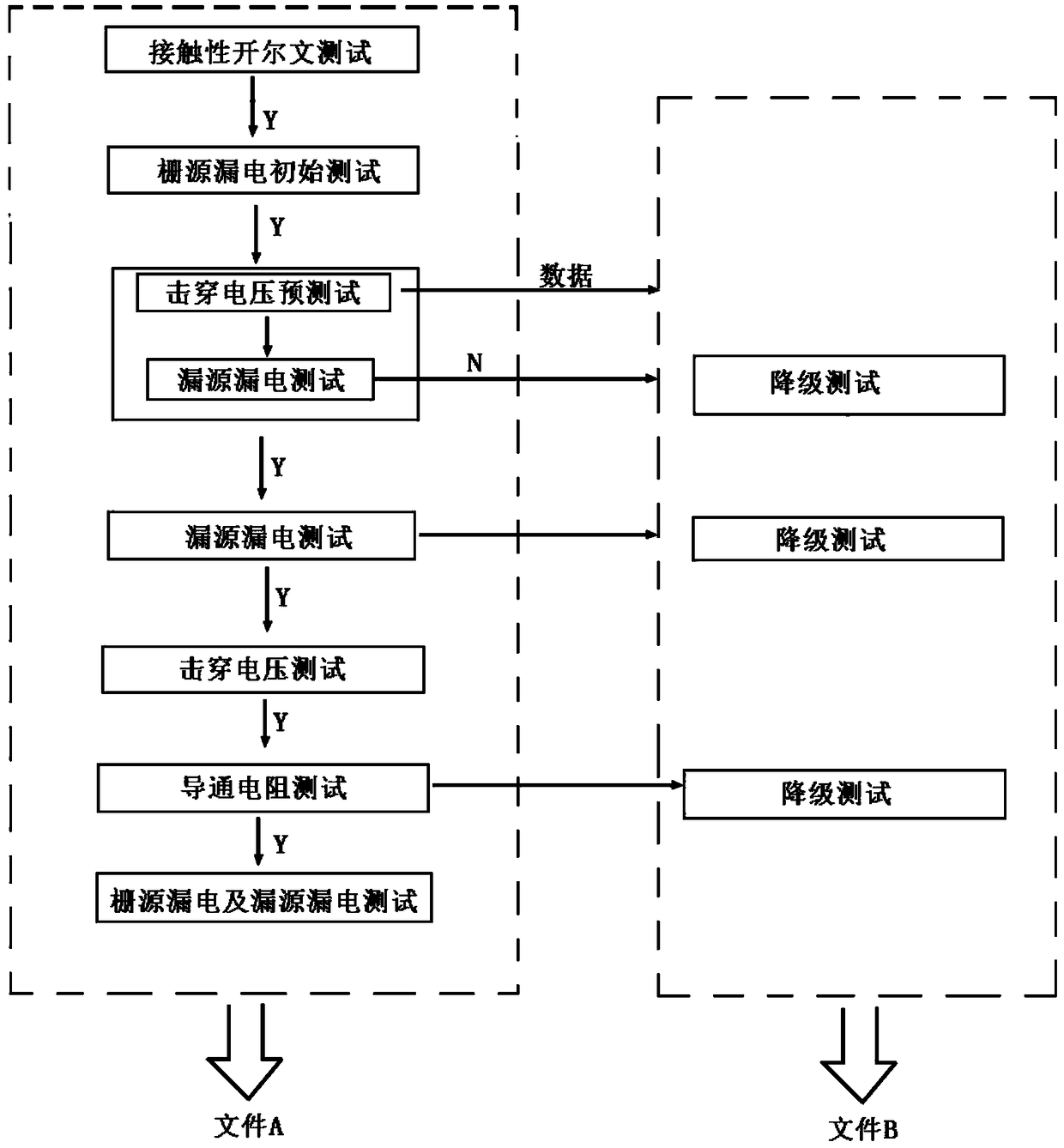
[0025] A test method of a super junction device according to the present invention, such as figure 2 As shown, the first step is to create two test data files before the test program starts, marked as file A and file B; the file A is used to record the data passed by the first-level test, and the file B is used to record the passed data of the second-level test The data. According to the actual situation, there may also be three-level tests, four...


PUM


Abstract

The invention discloses a test method for a super junction device. The method comprises steps that two test data files are established before the start of the test procedure; a contact Kelvin test isperformed; a chip passing the test is subjected to the next test; an initial gate and source leakage test is performed, and the test result IGSS0 is outputted to a file A; a drain and source leakage test is performed, firstly, the breakdown voltage pre-test is performed, a breakdown voltage value of a device is tested under the wide test condition, the drain and source leakage test is then performed, if the test result is not up to standards, the next jump downgrade test is performed; the drain and source leakage test condition is modified, the test is repeated; the breakdown voltage test is performed; the conductive on-resistance RDSON test is performed, screening is performed according to the standard test condition, and the test result is outputted to the file A; if the test does not pass the standard test condition, the jump downgrade test is performed; S8, the gate and source leakage test and the drain and source leakage test are repeated, and the test results IGSSF and IDSSF areoutputted to the file A; if the test does not pass, the chip is directly removed.

Description

technical field [0001] The invention relates to the field of manufacturing and testing of semiconductor devices, in particular to a super junction testing method. Background technique [0002] A large number of electronic components are used in electronic equipment, and various electronic components can be roughly divided into two categories: integrated circuits and super junctions. An integrated circuit, commonly known as a chip, is a tiny electronic device or component. Using a certain process, the transistors, resistors, capacitors, inductors and other components required in a circuit are interconnected, and they are fabricated on a small or several small semiconductor wafers or dielectric substrates, and then packaged in a tube. , become a microstructure with specific circuit functions. Most of today's semiconductor industry uses silicon-based integrated circuits. The super junction is a traditional single-package resistor, capacitor, inductor, power MOS and other bas...

Claims


Application Information

Patent Timeline
IPC IPC(8): G01R31/26
CPCG01R31/2601
Inventor 李晶晶谢晋春辛吉升
Owner SHANGHAI HUAHONG GRACE SEMICON MFG CORP
Why Eureka
Try Eureka