Fine line manufacturing method

A technology for fine circuits and circuit boards, which is used in chemical/electrolytic methods to remove conductive materials, printed circuits, and printed circuit manufacturing. The effect of small size, high machining accuracy and good insulation performance

Active Publication Date: 2019-02-01
武汉铱科赛科技有限公司
View PDF2 Cites 2 Cited by
  • Summary
  • Abstract
  • Description
  • Claims
  • Application Information

AI Technical Summary

Problems solved by technology

Greatly reducing the typesetting format can only greatly reduce the production capacity of COF and increase the production cost of COF

Method used


Image

  • Fine line manufacturing method
  • Fine line manufacturing method
  • Fine line manufacturing method

Examples


Embodiment Construction

[0048] The principles and features of the present invention are described below in conjunction with the accompanying drawings, and the examples given are only used to explain the present invention, and are not intended to limit the scope of the present invention.

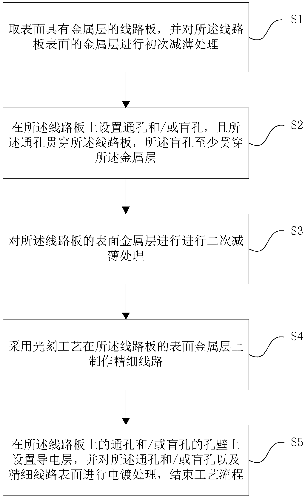
[0049] Such as figure 1 As shown, a method for making a fine circuit comprises the following steps:

[0050] Step 1: Take a circuit board with a metal layer on the surface, and perform initial thinning treatment on the metal layer on the surface of the circuit board;

[0051] Step 2: setting through holes and / or blind holes on the circuit board, and the through holes penetrate the circuit board, and the blind holes penetrate at least the metal layer on one side of the circuit board;

[0052] Step 3: performing secondary thinning treatment on the surface metal layer of the circuit board;

[0053] Step 4: using a photolithography process to fabricate fine circuits on the surface metal layer of the circuit board.

...


PUM


Abstract

The invention relates to a fine line manufacturing method. A metal layer in the surface of a circuit board is thinned preliminarily; the circuit board is provided with a through hole and/or a blind hole, the through hole penetrates the circuit board, and the blind hole penetrates the metal layer at least; the metal layer in the surface of the circuit board is thinned secondarily; a fine line is made on the surface metal layer of the circuit board via a photoetching process; and the hole wall(s) of the through hole and/or the blind hole in the circuit board is/are provided with a conducting layer, and the surfaces of the through hole and/or the blind hole and the fine line are electro-plated. The relatively thick circuit board material is thinned preliminarily to reduce the aperture thickness ratio, so that the micro hole can be bored in the circuit board; the bored circuit board is thinned secondarily, so that the thickness of the conductive metal layer in the surface is further reduced, and photoetching of the fine line is made possible; and prejudice in the industry is overcome, the cost is reduced greatly, deformation of the circuit board is relatively low due to support intensity of the metal layer, and the hole precision is higher.

Description

technical field [0001] The invention relates to the technical field of circuit board processing, in particular to a method for manufacturing fine circuits. Background technique [0002] COF (Chip On Flex, or, Chip On Film), often called chip-on-film, is to fix the driver IC on the flexible circuit board. It uses the flexible circuit board as the carrier of the packaged chip, and connects the chip to the flexible substrate circuit. technology. The so-called flexible circuit board, that is, a thin and flexible circuit board, usually uses copper foil as the base material, and is now widely used in digital products such as mobile phones and tablet computers. The flexible packaging substrate (COF) business has a high technical content. FPC only prints wires on the soft board, but COF packages the chip on the soft board. [0003] COF is an IC packaging technology. It uses the flexible substrate circuit FPC as the carrier of the packaged chip. ) for bonding (Bonding) technology....

Claims


Application Information

Patent Timeline
Patent Type & Authority Applications(China)
IPC IPC(8): H05K3/22H05K3/00H05K3/06
CPCH05K3/0094H05K3/06H05K3/22
Inventor 张立国
Owner 武汉铱科赛科技有限公司
Why Eureka
Try Eureka