A planar insulated gate bipolar transistor and its preparation method
A technology of bipolar transistors and insulated gates, applied in the direction of transistors, semiconductor/solid-state device manufacturing, semiconductor devices, etc., can solve the deterioration of forward voltage drop and turn-off loss compromise characteristics, increase forward voltage drop, increase device Drift region and other issues to achieve the effect of enhancing the conductance modulation effect, reducing the turn-on voltage drop, and optimizing the turn-off loss
- Summary
- Abstract
- Description
- Claims
- Application Information
AI Technical Summary
Problems solved by technology
Method used
Image
Examples
Embodiment 1
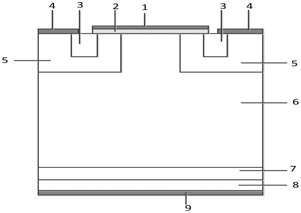
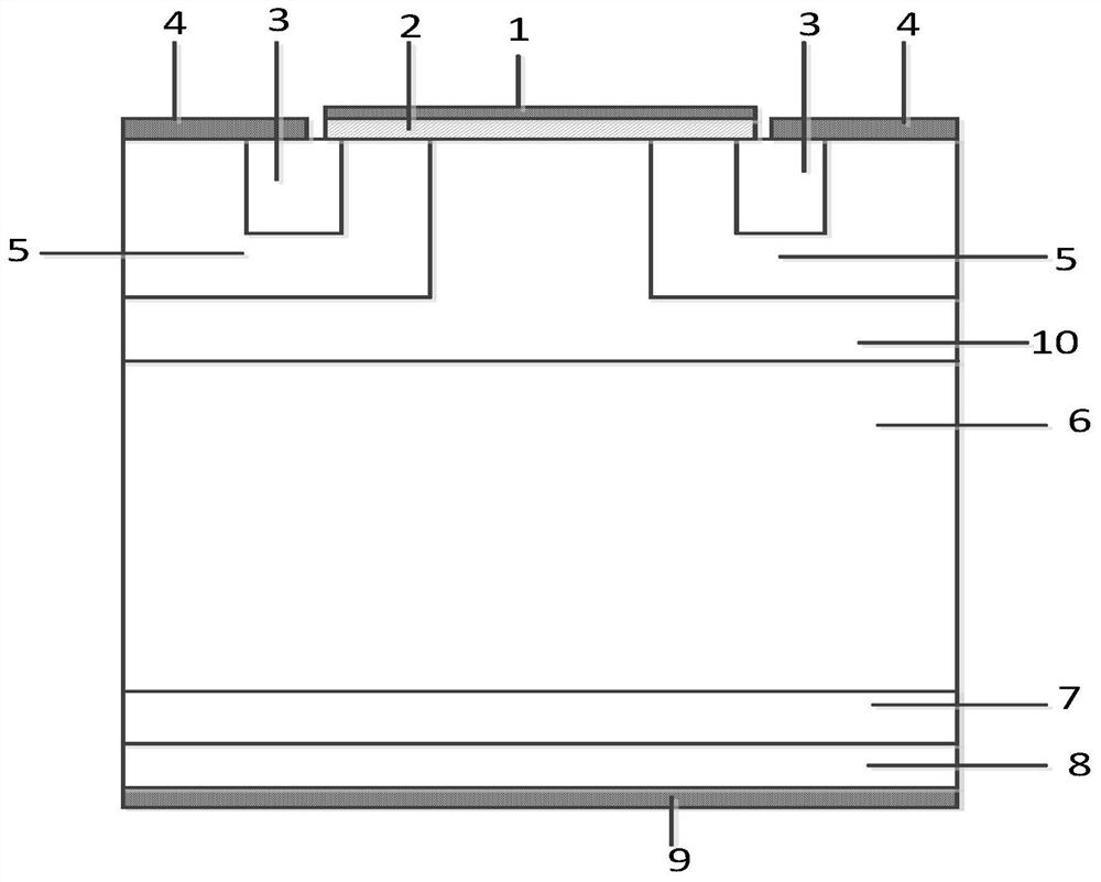
[0044] This embodiment provides a silicon carbide planar insulated gate bipolar transistor, including: a metallized collector 9, a P-type collector region 8, an N-type electric field stop layer 7, an N-drift region 6, and a P-type base region 5 , N+ emitter region 3, planar gate structure and emitter metal 4; metallized collector electrode 9 is located on the back of P-type collector region 8, N-type electric field stop layer 7 is located on the front of P-type collector region 8, N-type electric field stop Layer 7 is located on the front of the N-drift region 6; the P-type base region 5 is located on both sides of the top layer of the N-drift region 6; the N+ emitter region 3 is located on the top layer of the P-type base region 5, and is separated from the N-drift region 6 P-type base region 5; the upper surface of the P-type base region 5 between the N+ emitter regions 3 on both sides and part of the upper surface of the N+ emitter region 3 have a planar gate structure; on t...
Embodiment 2
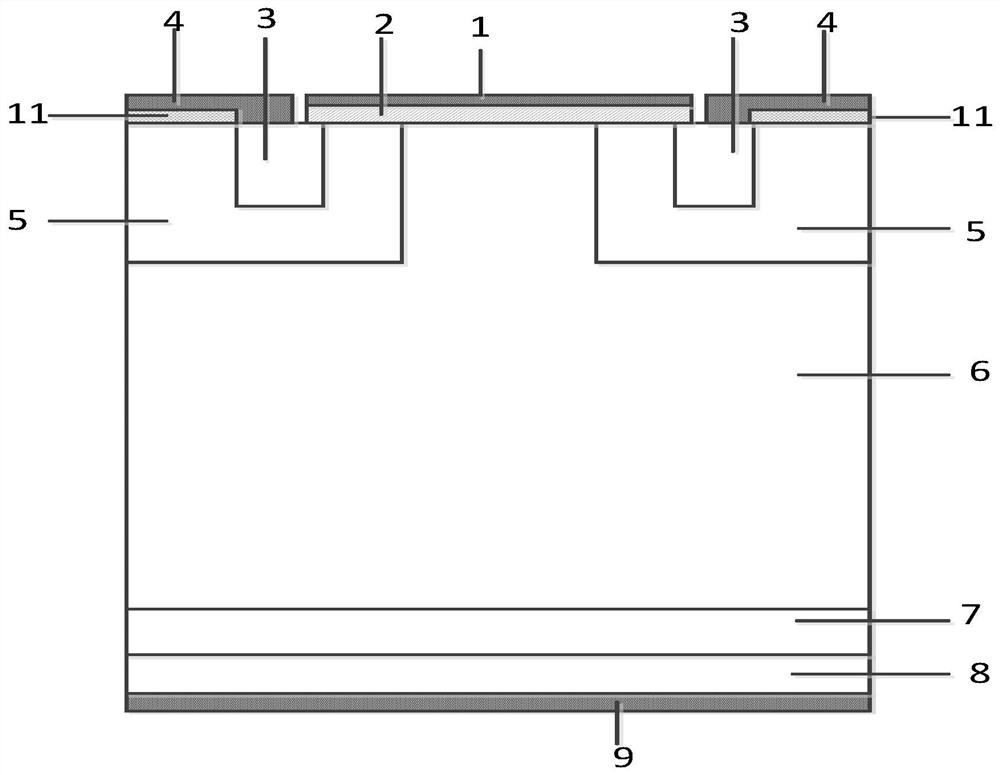
[0050] This embodiment provides a silicon carbide planar insulated gate bipolar silicon carbide transistor, the cell structure of which is as follows Figure 4 As shown, on the basis of Example 1, the P-type silicon layer 11 can also extend to the lower P-type base region 5 to form a trench structure, and the P-type silicon layer 11 is connected to the P-type silicon layer at the bottom and side walls of the trench. The P-type base region 5 and the N-type emitter region 3 form a heterojunction; the trench depth of the P-type silicon layer 11 may be the same as that of the N+ emitter region 3 or may be different.
[0051] Compared with Embodiment 1, this embodiment reduces the parasitic resistance formed in the P-type base region 5, reduces the voltage drop formed by the hole current in the P-type base region 5, and further suppresses the possible dynamic latch of the device. lock, which improves the high current shutdown capability of the device.
Embodiment 3
[0053] This embodiment provides a silicon carbide planar insulated gate bipolar silicon carbide transistor, the cell structure of which is as follows Figure 5 As shown, on the basis of Embodiment 2, the lower part of the P-type silicon layer 11 may also be a heavily doped P-type contact region 12, and the concentration of the P-type contact region 12 is greater than that of the P-type base region 5. concentration; the P-type silicon layer 11 and the P-type contact region 12 form a heterojunction.
[0054] Compared with Example 2, the concentration of the heavily doped P-type contact region 12 is much higher than that of the P-type base region 5, thereby forming a higher hole barrier, which can further increase the potential of the P-type base region and enhance the conductance modulation effect.
PUM
| Property | Measurement | Unit |
|---|---|---|
| thickness | aaaaa | aaaaa |
| thickness | aaaaa | aaaaa |
| thickness | aaaaa | aaaaa |
Abstract
Description
Claims
Application Information
 - R&D
- Intellectual Property
- Life Sciences
- Materials
- Tech Scout
- Unparalleled Data Quality
- Higher Quality Content
- 60% Fewer Hallucinations
Browse by: Latest US Patents, China's latest patents, Technical Efficacy Thesaurus, Application Domain, Technology Topic, Popular Technical Reports.
© 2025 PatSnap. All rights reserved.Legal|Privacy policy|Modern Slavery Act Transparency Statement|Sitemap|About US| Contact US: help@patsnap.com


