Semiconductor structure and forming method thereof

A semiconductor and gate structure technology, which is applied in semiconductor devices, semiconductor/solid-state device manufacturing, semiconductor/solid-state device components, etc., can solve the problems of semiconductor structure reliability to be improved, so as to reduce breakdown problems and improve reliability , the effect of increasing the distance

Active Publication Date: 2019-01-04
SEMICON MFG INT (SHANGHAI) CORP +1
View PDF3 Cites 9 Cited by
  • Summary
  • Abstract
  • Description
  • Claims
  • Application Information

AI Technical Summary

Problems solved by technology

[0005] With the reduction of device size, the reliability of the semiconductor structure formed by the existing technology needs to be improved

Method used


Image

  • Semiconductor structure and forming method thereof
  • Semiconductor structure and forming method thereof
  • Semiconductor structure and forming method thereof

Examples


Embodiment Construction

[0019] It can be seen from the background art that the semiconductor structure formed in the prior art has the problem of poor reliability. Now combine a semiconductor structure to analyze the reasons for its poor reliability:

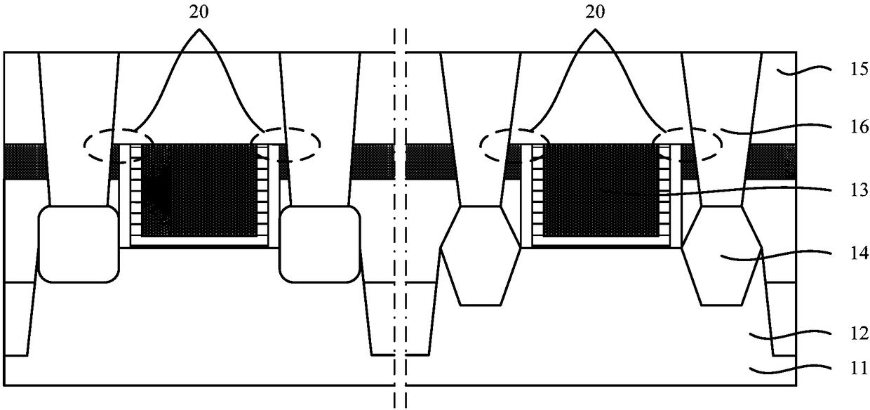
[0020] refer to figure 1 , shows a schematic cross-sectional structure of a semiconductor structure.

[0021] The semiconductor structure includes:

[0022] A substrate 11, having a fin 12 on the substrate 11; a metal gate structure 13, spanning the fin 12 and covering the surface of part of the top and part of the sidewall of the fin 12; source and drain doped regions, Including a stress layer 14, the stress layer 14 is located in the fin portion 12 on both sides of the metal gate structure 13; an interlayer dielectric layer 15 is located on the substrate 11, and covers the fin portion 12, the The stress layer 14 and the metal gate structure 13 ; the plug 16 , on the source-drain doped region, is electrically connected to the stress layer 14 , and ...


PUM


Abstract

A semiconductor structure and a forming method thereof are provided, wherein the forming method includes forming a substrate having a gate structure thereon; forming a first dielectric layer on the substrate; removing a portion of thickness of the first dielectric layer such that the top of the remaining first dielectric layer is lower than the top of the gate structure; and forming an isolation side wall is formed on the exposed side wall of the gate structure. The isolation side wall can effectively improve the electrical isolation performance between the gate structure and a plug formed subsequently, which is conducive to reducing the problem of breakdown between the gate structure and the plug, and is conducive to improving the reliability of the formed semiconductor structure.

Description

technical field [0001] The invention relates to the field of semiconductor manufacturing, in particular to a semiconductor structure and a forming method thereof. Background technique [0002] With the development of integrated circuits to ultra-large-scale integrated circuits, the circuit density inside the integrated circuit is increasing, and the number of components contained in the integrated circuit is also increasing, and the size of the components is also reduced. As the size of the semiconductor structure decreases, the channel of the device in the semiconductor structure shortens accordingly. Due to the shortening of the channel, the gradual channel approximation is no longer valid, and various unfavorable physical effects (especially the short channel effect) are highlighted, which degrades the performance and reliability of the device and limits the further reduction of the device size. [0003] In order to control the short channel effect, the further reduction...

Claims


Application Information

Patent Timeline
Patent Type & Authority Applications(China)
IPC IPC(8): H01L21/28H01L21/768H01L23/528H01L29/51
CPCH01L21/28247H01L21/76895H01L23/5283H01L29/518H01L21/76224H01L29/66545H01L29/0847H01L29/165H01L29/7848H01L29/785H01L27/0924H01L21/823821H01L29/66795H01L29/66568H01L29/78H01L21/0217H01L29/0649H01L21/762
Inventor 周飞
Owner SEMICON MFG INT (SHANGHAI) CORP
Why Eureka
Try Eureka