A tkd Determination Method for Single Grain Stress State of Polycrystalline Material
A polycrystalline material, stress state technology, applied in the analysis of materials, material analysis using radiation, material analysis using radiation diffraction, etc., can solve the problem that the stress state of grains cannot be determined, and the microscopic driving force cannot be known.
- Summary
- Abstract
- Description
- Claims
- Application Information
AI Technical Summary
Problems solved by technology
Method used
Image
Examples
Embodiment 1
[0037] Zr-4 alloy, whose nominal composition is Zr-1.5Sn-0.2Fe-0.1Cr, has excellent corrosion resistance and is widely used as cladding material for pressurized water reactors and heavy water reactors.
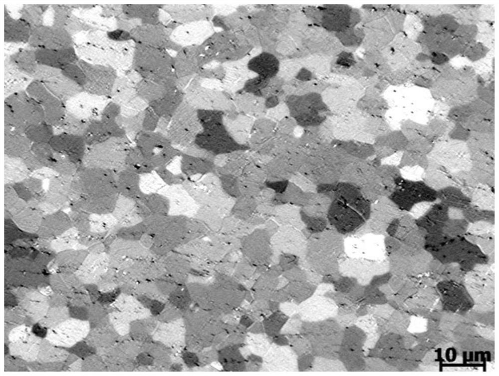
[0038] A Zr-4 alloy plate with a thickness of 4 mm has an average diameter of equiaxed α grains at room temperature of about 8 μm, and its microstructure is as follows: figure 2shown. After the alloy plate is sheared and deformed (please refer to the patent with publication number CN107044941A for the specific method), a thin slice sample is taken in the deformation zone, pre-ground to a thickness of 60 μm, and then punched (with a diameter of Ф3 mm), and the sample is ground again. The thickness is reduced to 40 μm, and finally double-jet electrolysis is used to reduce the thickness again. The electrolytic polishing solution adopts 10% perchloric acid and 90% alcohol by volume. With this, transmission sample preparation ends.
[0039] Using a transmission electron microsco...
Embodiment 2
[0046] A 45# steel bar with a diameter of 8mm. After the alloy undergoes compression deformation, the amount of compression deformation is 5%. Take a thin slice sample in the deformation zone, pre-grind to a thickness of 60 μm, then punch a hole (diameter Ф3mm), grind again, and thin the sample to 40 μm, and finally double-jet electrolysis thins again, and the volume fraction of the electrolytic polishing solution is 10 % perchloric acid and 90% alcohol. With this, transmission sample preparation ends.
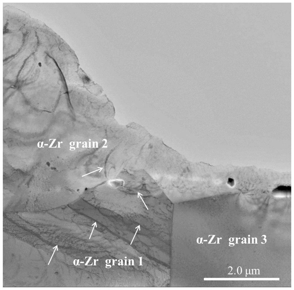
[0047] as attached Figure 8 As shown, the dislocation densities in the three grains at the edge of the hole in the transmission sample have an order of magnitude difference, as indicated by the arrows in the figure. Grain 1 (hereinafter referred to as grain 1) has the highest dislocation density, followed by Grain 2 (hereinafter referred to as grain 2), and Grain 3 (hereinafter referred to as grain 3) basically has no dislocation contrast inside the grain, that is, the gra...
Embodiment 3
[0052] A pure copper TU0 plate with a thickness of 5mm. After the alloy sheet is stretched and deformed, a thin slice sample is taken in the deformed area, pre-ground to a thickness of 60 μm, then punched (diameter Ф3mm), ground again, and the sample is thinned to 40 μm, and finally thinned again by double-jet electrolysis . With this, transmission sample preparation ends.
[0053] as attached Figure 11 As shown, in the STEM mode, it is observed that the dislocation densities in the three grains differ by orders of magnitude, as indicated by the arrows in the figure. The dislocation densities inside Grain 2 (hereinafter referred to as grain 2) and Grain 3 (hereinafter referred to as grain 3) are basically the same, and the dislocation density inside Grain 1 (hereinafter referred to as grain 1) is significantly lower than that of grain 2 and grain 3. According to the dislocation densities inside the three grains, it can be inferred that grain 2 and grain 3 are in soft orie...
PUM
| Property | Measurement | Unit |
|---|---|---|
| thickness | aaaaa | aaaaa |
| diameter | aaaaa | aaaaa |
| diameter | aaaaa | aaaaa |
Abstract
Description
Claims
Application Information
 - R&D
- Intellectual Property
- Life Sciences
- Materials
- Tech Scout
- Unparalleled Data Quality
- Higher Quality Content
- 60% Fewer Hallucinations
Browse by: Latest US Patents, China's latest patents, Technical Efficacy Thesaurus, Application Domain, Technology Topic, Popular Technical Reports.
© 2025 PatSnap. All rights reserved.Legal|Privacy policy|Modern Slavery Act Transparency Statement|Sitemap|About US| Contact US: help@patsnap.com


