A trench-gate dmos device with a dielectric barrier

A dielectric barrier and gate dielectric layer technology, applied in semiconductor devices, electrical components, circuits, etc., can solve problems such as the inability to eliminate parasitic BJT turn-on, the inability to infinitely reduce the parasitic BJT base resistance, and increase the device threshold voltage. Effects of UIS failure capability, improved UIS tolerance, and improved reliability

Active Publication Date: 2021-03-30
UNIV OF ELECTRONICS SCI & TECH OF CHINA
View PDF5 Cites 0 Cited by
  • Summary
  • Abstract
  • Description
  • Claims
  • Application Information

AI Technical Summary

Problems solved by technology

However, this method cannot prevent the turn-on of parasitic BJT, and it cannot avoid the active failure mode of device UIS caused by avalanche breakdown; in addition, it can only be reduced to a certain extent by high-energy boron implantation or deep diffusion. The base resistance cannot infinitely reduce the base resistance of the parasitic BJT, otherwise it will increase the threshold voltage of the device

Method used


Image

  • A trench-gate dmos device with a dielectric barrier
  • A trench-gate dmos device with a dielectric barrier
  • A trench-gate dmos device with a dielectric barrier

Examples


Embodiment 1

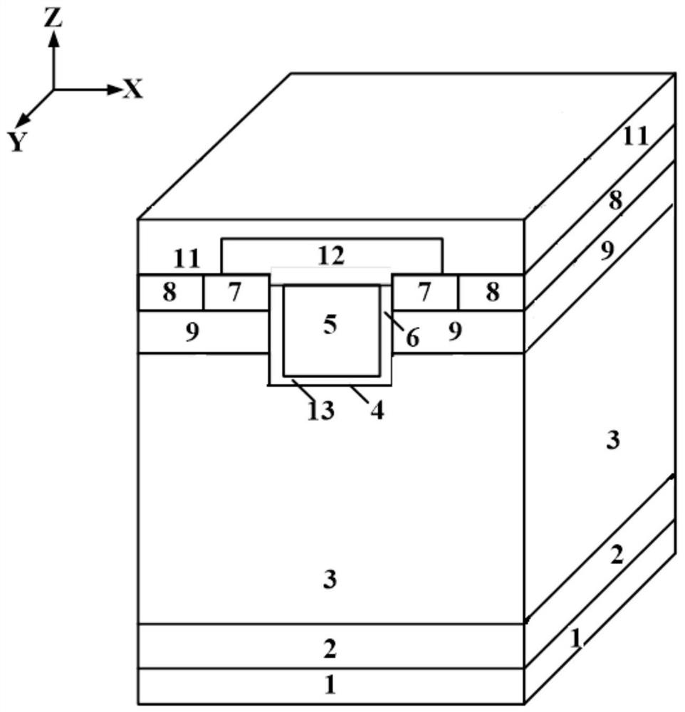
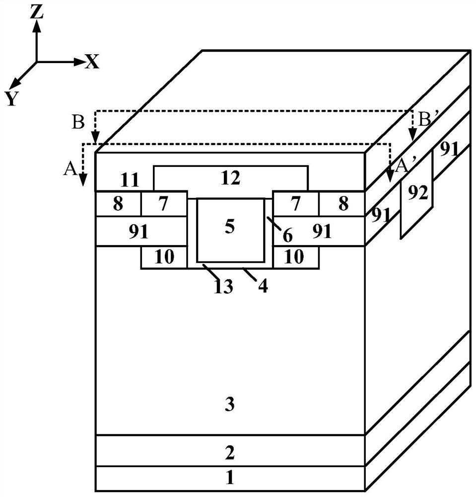
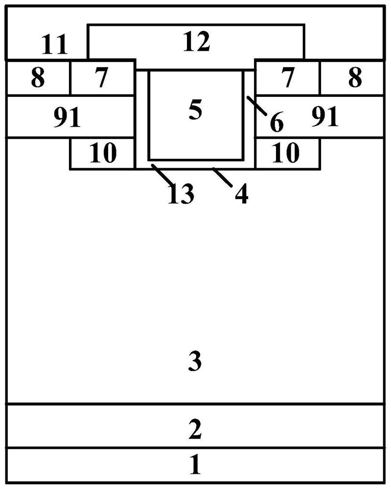
[0024] This embodiment provides a trench gate DMOS device with a dielectric barrier layer, the three-dimensional schematic diagram of its cell structure is as follows figure 2 As shown, the schematic diagrams of the sections obtained along the cell structure line AA' and BB' are as follows image 3 with Figure 4 As shown, it includes a metallized drain 1, a first conductivity type semiconductor doped substrate 2, a first conductivity type semiconductor doped drift region 3, a gate electrode 5, a gate dielectric layer 6, a second conductivity type semiconductor body region, and a second conductivity type semiconductor body region. A semiconductor doped source region 7 of one conductivity type, a semiconductor doped contact region 8 of a second conductivity type and a metallized source 11;

[0025]The metallized drain 1 is located on the back side of the first conductivity type semiconductor doped substrate 2; the first conductivity type semiconductor doped drift region 3 is ...


PUM


Abstract

A trench gate DMOS device with a dielectric barrier layer belongs to the technical field of power semiconductors. Based on the structure of the traditional trench-gate DMOS device, the present invention alternately arranges body regions with different doping concentrations and junction depths below the source region and the contact region along the trench extension direction, and there are also shallow junctions and high-concentration body regions below the body region. The dielectric barrier layer corresponding to the position of the source region is set to isolate the current path under the source region, and then guide the avalanche current to avoid the shallow junction and high-concentration body region, and flow away directly through the contact region, thus preventing the parasitic BJT open. The present invention works by blocking the turn-on of the parasitic BJT. The UIS tolerance of the device is improved, thereby improving the anti-UIS failure capability of the device. At the same time, because there is no dielectric barrier layer under the deep junction and low-concentration body region, when the device is conducting forward, the carrier current can still flow out through the inversion deep junction and low-concentration body region, so the conduction characteristics of the device and Threshold voltage is not negatively affected.

Description

technical field [0001] The invention belongs to the technical field of power semiconductors, and in particular relates to a trench gate DMOS device with a dielectric barrier layer. Background technique [0002] Power semiconductor devices are essential core devices for realizing power conversion and control. Power MOSFET has become the most widely used power device because of its fast switching speed, low loss, high input impedance, low driving power, and good frequency characteristics. The system application of power MOSFET requires that it has lower power loss and higher reliability under high electrical stress. Therefore, reliability is very important for the system application of power MOSFET. The research shows that the failure of the device in the dynamic process is higher than the failure in the static process, and the failure mechanism is more complicated. The switching process (Unclamped Inductive Switching, UIS) under the unclamped inductive load is generally co...

Claims


Application Information

Patent Timeline
Patent Type & Authority Patents(China)
IPC IPC(8): H01L29/78H01L29/06
CPCH01L29/0634H01L29/7813
Inventor 任敏杨梦琦王梁浩李泽宏高巍张金平张波
Owner UNIV OF ELECTRONICS SCI & TECH OF CHINA
Why Eureka
Try Eureka