A thermoelectric component having a wrapping body structure
A technology for components and cladding, which is applied in the directions of thermoelectric device parts, thermoelectric device manufacturing/processing, thermoelectric device node lead wire materials, etc., and can solve the problems of low stability and oxidation resistance.
- Summary
- Abstract
- Description
- Claims
- Application Information
AI Technical Summary
Problems solved by technology
Method used
Image
Examples
Embodiment 1
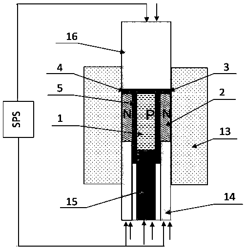
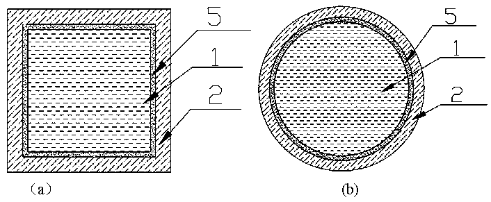
[0061] This embodiment 1 is to prepare CoSb with coating structure 3 Base-filled skutterudite devices. The nominal composition of the P-type material is CeFe 4 Sb 12 , the nominal composition of N-type material is Yb 0.3 co 4 Sb 12 , where CeFe 4 Sb 12 As core material P, Yb 0.3 co 4 Sb 12 As the outer cladding material N. In this example, a circular sintering mold is taken as an example, and the inner diameter of the mold is 10mm. First put the mold annular lower ram 14 and the mold lower ram 15 in the outer mold cover 13, and put the insulating material 5 between the mold annular lower ram 14 and the mold lower ram 15, and form the insulating material 5 Put a mold lower pressure head 15 into the cavity equally, adjust the position of the mold annular lower pressure head 14, the mold lower pressure head 15 and the insulating material 5 in the outer mold casing 13, so that the height of the insulating material 5 is higher than the outer mold casing 13, In the cavit...
Embodiment 2
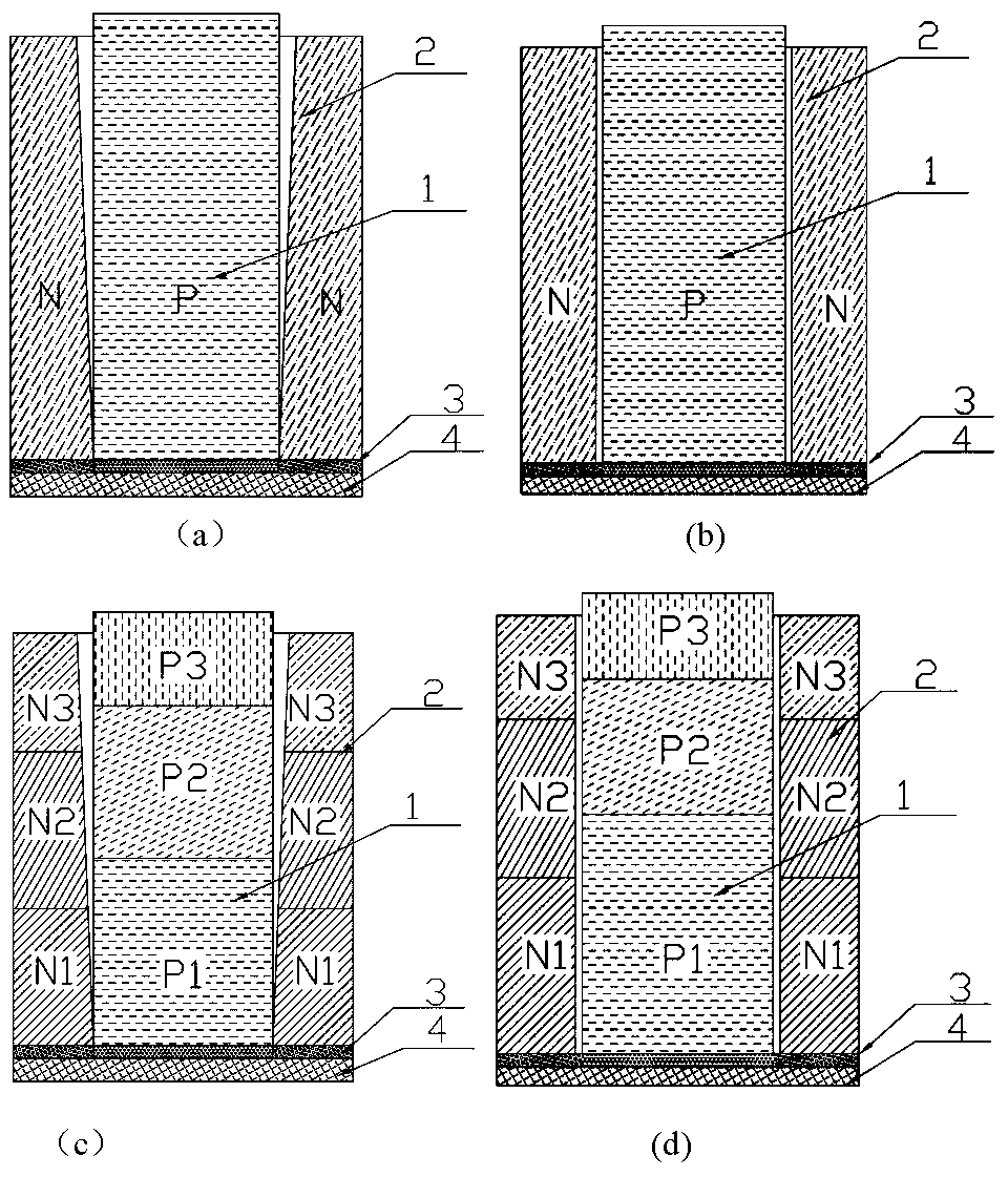
[0063] This embodiment is to prepare a thermoelectric device with a two-stage structure and a wrapping structure. The nominal composition of the P-type material is FeNbSb-based and CeFe 4 Sb 12 The base P-type thermoelectric material, the nominal composition of the N-type material is ZrNiSn base and Yb 0.3 co 4 Sb 12 , where ZrNiSn base and Yb 0.3 co 4 Sb 12 As external cladding materials N, FeNbSb-based and CeFe 4 Sb 12 The base P-type thermoelectric material is used as the core material P. In this example, the circular sintering mold is taken as an example, first use such as figure 1 The molds shown were sintered separately, such as Figure 4 The structures shown are P-type and N-type components with electrodes. First put the mold annular lower ram 14 and the mold lower ram 15 in the outer mold cover 13, and put the insulating material 5 between the mold annular lower ram 14 and the mold lower ram 15, and form the insulating material 5 Put a mold lower pressure h...
PUM
| Property | Measurement | Unit |
|---|---|---|
| thickness | aaaaa | aaaaa |
| thickness | aaaaa | aaaaa |
| thickness | aaaaa | aaaaa |
Abstract
Description
Claims
Application Information
 - R&D
- Intellectual Property
- Life Sciences
- Materials
- Tech Scout
- Unparalleled Data Quality
- Higher Quality Content
- 60% Fewer Hallucinations
Browse by: Latest US Patents, China's latest patents, Technical Efficacy Thesaurus, Application Domain, Technology Topic, Popular Technical Reports.
© 2025 PatSnap. All rights reserved.Legal|Privacy policy|Modern Slavery Act Transparency Statement|Sitemap|About US| Contact US: help@patsnap.com


