VCSEL-APD integrated chip and a preparation method thereof
A technology of integrating chips and structural layers, applied in the field of detection, can solve the problems of low integration of lasers and detectors, and achieve the effects of high integration, increased laser flux, and increased aperture ratio.
- Summary
- Abstract
- Description
- Claims
- Application Information
AI Technical Summary
Problems solved by technology
Method used
Image

Examples
Embodiment 1
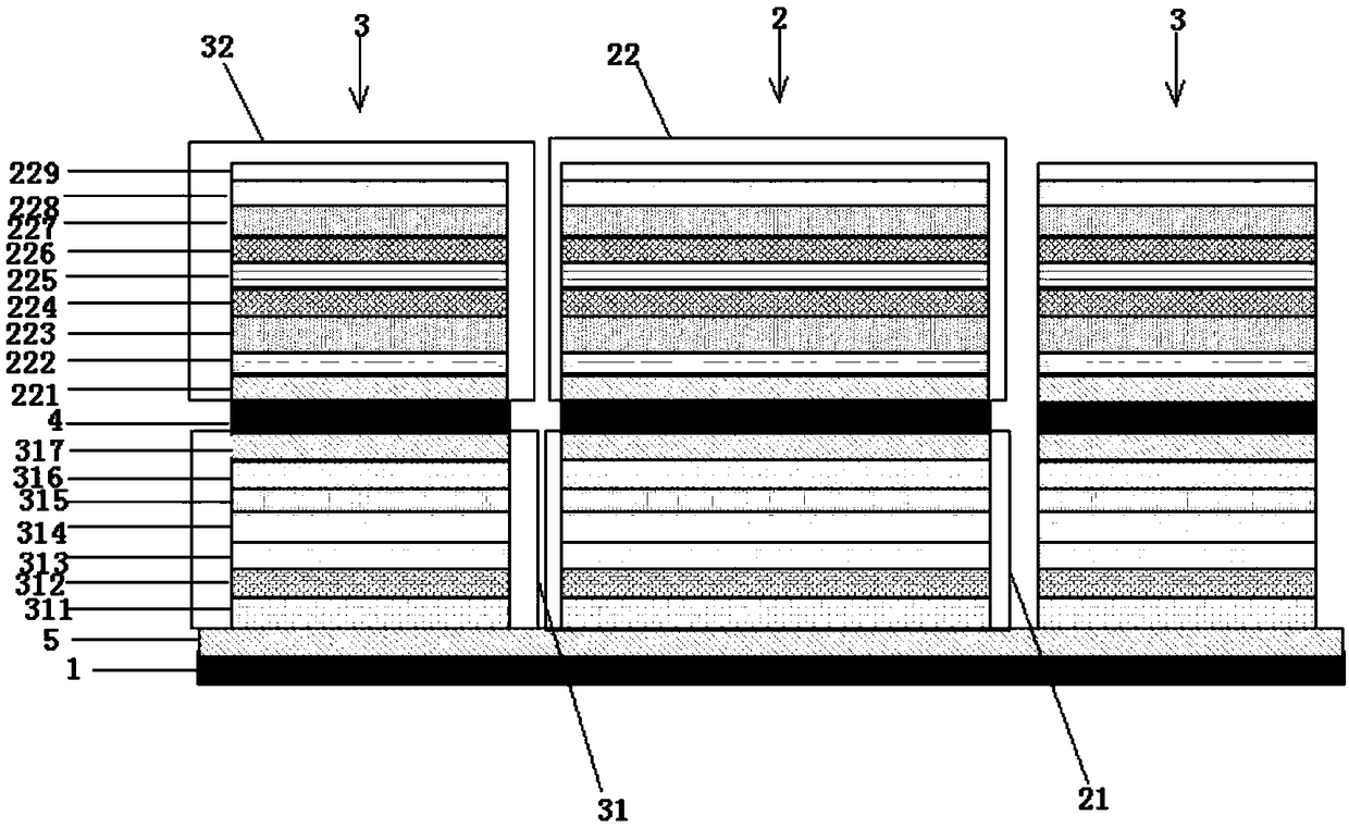
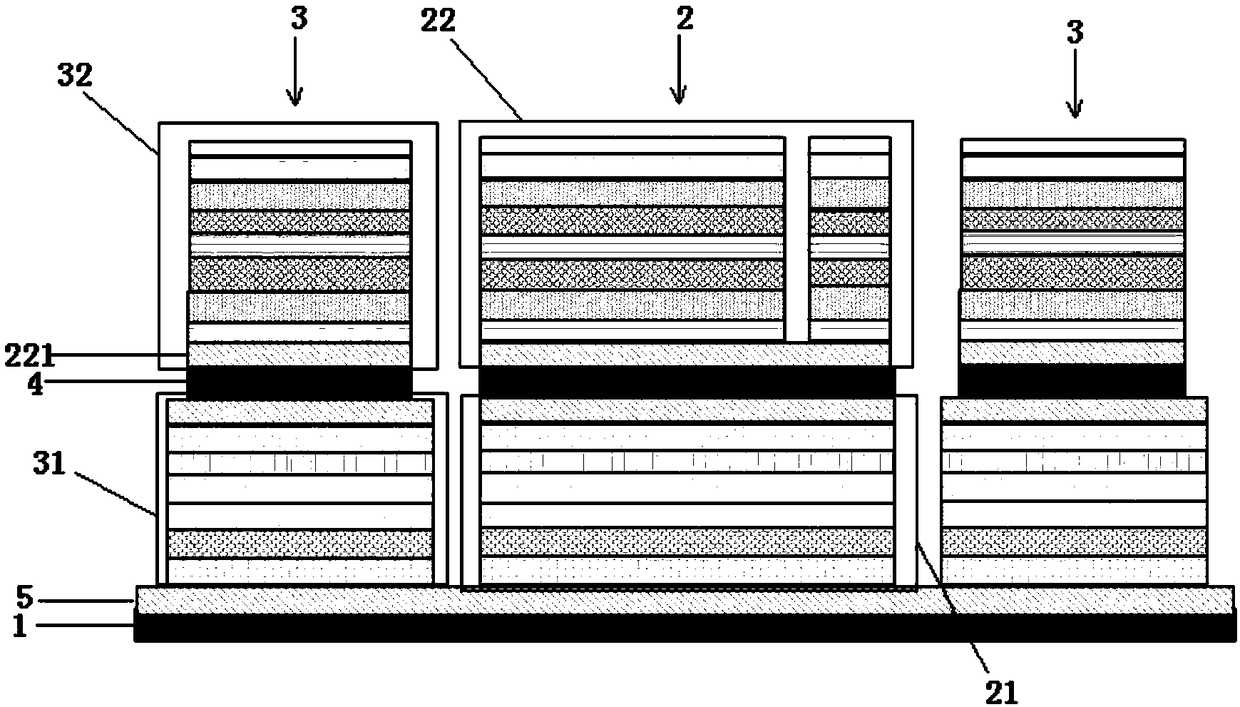
[0054] The embodiment of the present invention provides a VCSEL and APD integrated chip, such as Figure 1-9 As shown, a substrate 1 is included, and a signal transmitting unit 2 and a signal receiving unit 3 distributed along the horizontal direction and separated from each other are arranged on the substrate 1; the signal transmitting unit 2 includes a first signal stacked on the substrate 1 The receiving structure layer 21 and the first signal transmitting structure layer 22 ; the signal receiving unit 3 includes a second signal receiving structure layer 31 and a second signal transmitting structure layer 32 stacked on the substrate 1 .
[0055] In this embodiment, the first signal transmitting structure layer 22 in the signal transmitting unit 2 and the second signal transmitting structure layer 32 in the signal receiving unit 3 are preferably vertical cavity surface emitting laser (VCSEL) structures. The first signal receiving structure layer 21 in the signal transmitting...
Embodiment 2
[0088] The embodiment of the present invention provides a method for preparing a VCSEL and APD integrated chip, comprising the following steps:
[0089] Step S21, forming a number of signal transmitting units 2 and signal receiving units 3 separated from each other on the substrate 1, the signal transmitting unit 2 includes a first signal receiving structure layer 21 and a first signal transmitting structure layer 22 arranged in layers, and the signal receiving unit The unit 3 includes a second signal receiving structure layer 31 and a second signal emitting structure layer 32 that are stacked, wherein the first signal receiving structure layer 21 and the second signal receiving structure layer 31 are both avalanche photodiodes ( APD) structure layer, and prepared in the same layer, the first signal emission structure layer 22 and the second signal emission structure layer 32 are vertical cavity surface emitting laser (VCSEL) structure layers, and prepared in the same layer.
...
Embodiment 3
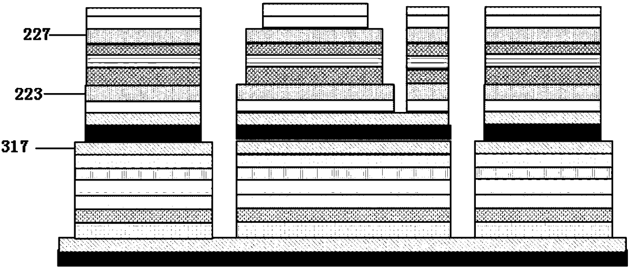
[0114] The embodiment of the present invention provides a specific example of the preparation method of the VCSEL and APD integrated chip provided in the above-mentioned embodiment 2. Include the following steps:
[0115] Step 1: sequentially forming a buffer layer, an avalanche photodiode (APD) structure layer, an intermediate barrier layer and a vertical cavity surface emitting laser (VCSEL) structure layer on a P-InP substrate. Concrete structure and material are with embodiment 1. Thick silicon nitride (SiN) X ) as a mask, etch to the top of the P-InP buffer layer, form a cylindrical mesa of InGaAs APD on the front, and form the pattern and registration mark of the APD array on the back of the InP substrate (see figure 1 ).
[0116] Step 2: Utilize the ICP dry etching method configured with the OES function, use silicon nitride as a mask, etch to the top of the contact layer, and form the N-type lower electrode contact layer step of the APD (see figure 2 ).
[0117]...
PUM
 Abstract
Description
Claims
Application Information
 - R&D
- Intellectual Property
- Life Sciences
- Materials
- Tech Scout
- Unparalleled Data Quality
- Higher Quality Content
- 60% Fewer Hallucinations
Browse by: Latest US Patents, China's latest patents, Technical Efficacy Thesaurus, Application Domain, Technology Topic, Popular Technical Reports.
© 2025 PatSnap. All rights reserved.Legal|Privacy policy|Modern Slavery Act Transparency Statement|Sitemap|About US| Contact US: help@patsnap.com