A kind of preparation method of stainless steel substrate thick film heating element
A heating element, stainless steel technology, applied in electrical elements, electric heating devices, ohmic resistance heating and other directions, can solve the problems of low production efficiency, high energy consumption, high raw material requirements, improve production efficiency, improve qualification rate, reduce energy consumption Effect
- Summary
- Abstract
- Description
- Claims
- Application Information
AI Technical Summary
Problems solved by technology
Method used
Image
Examples
Embodiment 1
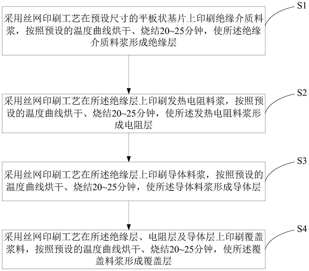
[0020] Please refer to figure 1 , the invention provides a method for preparing a thick film heating element with a stainless steel substrate, comprising the following steps:
[0021] Step S1, using a screen printing process to print insulating dielectric slurry on a flat substrate with a preset size, drying and sintering for 20 to 25 minutes according to a preset temperature curve, so that the insulating dielectric slurry forms an insulating layer;
[0022] Step S2, printing a heating resistor slurry on the insulating layer by using a screen printing process, drying and sintering for 20 to 25 minutes according to a preset temperature curve, so that the heating resistor slurry forms a resistance layer;
[0023] Step S3, using a screen printing process to print a conductor paste on the insulating layer, drying and sintering for 20 to 25 minutes according to a preset temperature curve, so that the conductor paste forms a conductor layer;
[0024] Step S4, printing a covering pa...
Embodiment 2
[0027] Said step 1 includes:
[0028] Step 11, using screen printing technology to print insulating dielectric slurry on a flat substrate with a preset size, drying and sintering for 20 to 25 minutes according to a preset temperature curve, so that the insulating dielectric slurry forms a first layer of insulation Floor;
[0029] Step 12: Print insulating dielectric slurry on the first insulating layer by screen printing process, dry and sinter according to a preset temperature curve for 20 to 25 minutes, so that the insulating dielectric slurry forms a second insulating layer Floor;
[0030] Step 13: Print insulating dielectric slurry on the second insulating layer by screen printing process, dry and sinter according to a preset temperature curve for 20 to 25 minutes, so that the insulating dielectric slurry forms a third insulating layer Floor;
[0031] Step 14: Print insulating dielectric slurry on the third insulating layer by screen printing process, dry and sinter acc...
Embodiment 3
[0047] The resistance layer comprises a plurality of strip-shaped resistance strips, and the resistance strips are arranged parallel to each other;
[0048] The conductor layer is made of silver, and is in the shape of a line and distributed on the insulating layer at intervals. One end of each conductor line is connected to the resistance band, and the other end is exposed outside the packaging layer for connecting with A conductive wire is soldered; said conductive wire is made of silver or copper;
[0049] Also includes:
[0050] Step 7, placing the connecting end of the conductive wire on the connecting end of the conductive wire;
[0051] Step 8, coating the nano-silver solder paste on the connecting end of the conductive wire and the connecting end of the conductive wire;
[0052] Step 9, heating the nano-silver solder paste by means of a rapid heating device to complete the welding of the conductive wire and the conductive wire. The rapid heating equipment includes one...
PUM
| Property | Measurement | Unit |
|---|---|---|
| particle size | aaaaa | aaaaa |
Abstract
Description
Claims
Application Information
 - R&D
- Intellectual Property
- Life Sciences
- Materials
- Tech Scout
- Unparalleled Data Quality
- Higher Quality Content
- 60% Fewer Hallucinations
Browse by: Latest US Patents, China's latest patents, Technical Efficacy Thesaurus, Application Domain, Technology Topic, Popular Technical Reports.
© 2025 PatSnap. All rights reserved.Legal|Privacy policy|Modern Slavery Act Transparency Statement|Sitemap|About US| Contact US: help@patsnap.com


