Manufacturing process of 6-layer microphone embedded circuit board with embedded chip

A technology of embedded chip and manufacturing process, applied in the direction of multi-layer circuit manufacturing, printed circuit manufacturing, printed circuit, etc., can solve the problems of limiting the space expansion and utilization rate of terminal products, and achieve favorable expansion, low cost investment, and improvement effect. Effect

Active Publication Date: 2019-12-06
JIANGSU PROVISION ELECTRONICS CO LTD
View PDF6 Cites 0 Cited by
  • Summary
  • Abstract
  • Description
  • Claims
  • Application Information

AI Technical Summary

Problems solved by technology

The thickness of the shell depends on the raised height of the chip on the carrier board after the chip is mounted, so this method limits the thinning of the microphone product thickness, and limits the expansion and utilization of the terminal product space; with the increasing number of terminal products The demand for thinner and thinner makes it urgent to realize the manufacturing process of microphone circuit boards that can be embedded and mounted chips

Method used


Image

  • Manufacturing process of 6-layer microphone embedded circuit board with embedded chip
  • Manufacturing process of 6-layer microphone embedded circuit board with embedded chip
  • Manufacturing process of 6-layer microphone embedded circuit board with embedded chip

Examples


Embodiment Construction

[0033] A preferred embodiment of the present invention will be described in detail below in conjunction with the accompanying drawings. However, the scope of protection of the present invention is not limited to the following examples, that is, any simple equivalent changes and modifications made based on the patent scope of the present invention and the content of the description are still within the scope of the patent of the present invention.

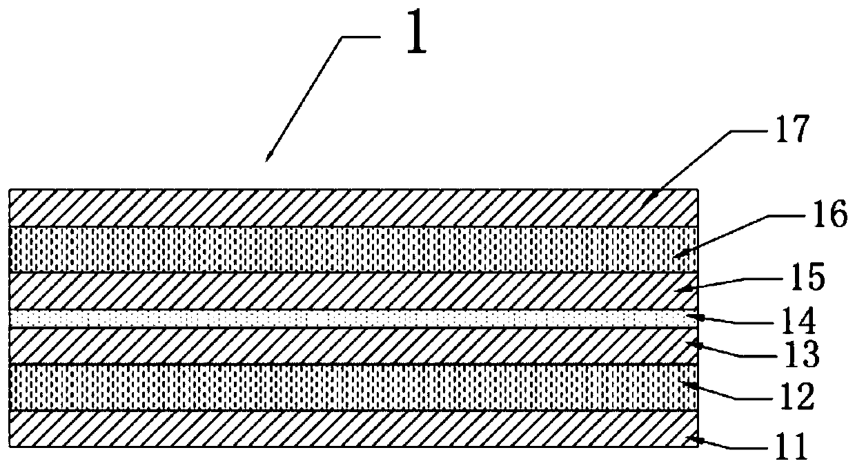
[0034] refer to Figure 1-7 , is a 6-layer microphone embedded circuit board manufacturing process for an embedded chip of the present invention, comprising the following steps:

[0035] Step 1, preparing a four-layer embedded substrate 1 that has been laminated and etched twice;

[0036] Step 2: Expose the double-sided laminated dry film of the four-layer embedded capacitor substrate, etch out the sub-outer layer pattern, and reserve the corresponding preset chip position on an outer layer copper foil of the four-layer embedded ca...


PUM


Abstract

The invention discloses a manufacturing process of a 6-layer microphone embedded circuit board of an embedded chip, which comprises the steps as follows: etching the double-sided layer of the four- embedded buried substrate to the outer layer pattern, a copper skin of the mounting chip is reserved on one outer copper foil corresponding to a preset chip position, etching the isolation ring around the copper skin; and obtaining a 6-layer embedded substrate, by pressing both sides of the4-layer embedded substrate sequentially to a layer of copper foil by a prepreg; etching out window pattern on the outermost copper foil of the 6-layer embedded substrate; burning grooves in 6-layer embedded substrate, and removing the adjacent prepreg layer corresponding to the window pattern to form a depth groove initial shape which can be embedded in the chip; drilling a sound hole on a 6-layer embedded substrate; exposing the double-sided adhesive dry film of the 6-layer embedded substrate to etch theouter layer, and meanwhile etching the copper on the bottom of the initial groove of the depth groove , to obtain a depth groove. The chip is embedded in the depth groove, which is, obtaining 6-layermicrophone embedded circuit board of embedded chip. According to the manufacturing process by the invention the problems of the difficult in thinning in traditional MEMS product are solved.

Description

technical field [0001] The invention relates to a manufacturing process of an embedded circuit board, in particular to a manufacturing process of a 6-layer microphone embedded circuit board with embedded chips. Background technique [0002] The chip around the sound hole of the finished microphone circuit board is designed in the same plane as other areas. Due to the limitation of the chip structure, it is currently difficult to reduce the thickness of the chip from the perspective of technology and cost. The calculation method of the overall microphone thickness after packaging is: the total thickness of the microphone circuit board + the thickness of the shell = the overall thickness of the microphone. The thickness of the shell depends on the raised height of the chip on the carrier board after the chip is mounted, so this method limits the thinning of the microphone product thickness, and limits the expansion and utilization of the terminal product space; with the increa...

Claims


Application Information

Patent Timeline
Patent Type & Authority Patents(China)
IPC IPC(8): H05K3/46
CPCH05K3/4644H05K3/4697H05K2201/10083
Inventor 马洪伟陆敏晨
Owner JIANGSU PROVISION ELECTRONICS CO LTD
Why Eureka
Try Eureka